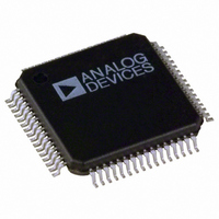
ADE7566ASTZF8 Analog Devices Inc, ADE7566ASTZF8 Datasheet - Page 110

ADE7566ASTZF8
Manufacturer Part Number
ADE7566ASTZF8
Description
IC ENERGY METER MCU 8K 64LQFP
Manufacturer
Analog Devices Inc
Datasheets
1.ADE7169ASTZF16.pdf
(152 pages)
2.ADE7566ASTZF8-RL.pdf
(136 pages)
3.ADE7169ASTZF16.pdf
(144 pages)
Specifications of ADE7566ASTZF8
Applications
Energy Measurement
Core Processor
8052
Program Memory Type
FLASH (8 kB)
Controller Series
ADE75xx
Ram Size
512 x 8
Interface
I²C, SPI, UART
Number Of I /o
20
Voltage - Supply
3.135 V ~ 3.465 V
Operating Temperature
-40°C ~ 85°C
Mounting Type
Surface Mount
Package / Case
64-LQFP
Ic Function
Single Phase Energy Measurement IC
Supply Voltage Range
3.13V To 3.46V, 2.4V To 3.7V
Operating Temperature Range
-40°C To +85°C
Digital Ic Case Style
LQFP
No. Of Pins
64
Lead Free Status / RoHS Status
Lead free / RoHS Compliant
Available stocks
Company
Part Number
Manufacturer
Quantity
Price
Company:
Part Number:
ADE7566ASTZF8
Manufacturer:
Analog Devices Inc
Quantity:
10 000
Company:
Part Number:
ADE7566ASTZF8-RL
Manufacturer:
Analog Devices Inc
Quantity:
10 000
ADE7116/ADE7156/ADE7166/ADE7169/ADE7566/ADE7569
ECON—Flash Control SFR
Programming flash memory is done through the Flash Control
SFR (ECON, Address 0xB9). This SFR allows the user to read,
write, erase, or verify the 16 kB of flash memory. As a method of
security, a key must be written to the FLSHKY, Address 0xBA)
to initiate any user access to the flash memory. Upon completion
of the flash memory operation, the FLSHKY SFR is reset such that
it must be written to before another flash memory operation.
Requiring the key to be set before an access to the flash memory
decreases the likelihood of user code or data being overwritten
by a runaway program.
Table 102. Flash Control SFR (ECON, Address 0xB9)
Bit
[7:0]
Table 103. Flash Key SFR (FLSHKY, Address 0xBA)
Bit
[7:0]
Table 104. Flash Protection Key SFR (PROTKY, Address 0xBB)
Bit
[7:0]
Table 105. Flash Data SFR (EDATA, Address 0xBC)
Bit
[7:0]
Mnemonic
FLSHKY
Mnemonic
PROTKY
Mnemonic
EDATA
Mnemonic
ECON
Default
0xFF
Default
0xFF
Default
0
Default
0
The content of this SFR is compared to the flash memory location at Address 0x3FFA. If the two values
match, the update of the write/erase and read protection setup is allowed (see the Protecting the Flash
section).
If the protection key in the flash is 0xFF, the PROTKY SFR value is not used for comparison. This SFR is
also used to write the protection key in the flash. This is done by writing the desired value in PROTKY
and by writing 0x08 in the ECON SFR. This operation can only be done once.
Description
The content of this SFR is compared to the flash key, 0x3B. If the two values match, the next ECON
operation is allowed (see the Protecting the Flash section).
Description
Description
Flash pointer data.
EADRH
Value
1
2
3
4
5
8
PROTECTION KEY
Figure 95. Flash Memory Read/Write/Erase Protection Block Diagram
FLSHKY
EADRL
ADDRESS
FLASH
Description
Write byte. The value in EDATA is written to the flash memory at the page address given by
EADRH (Address 0xC7) and EADRL (Address 0xC6). Note that the byte being addressed must be
pre-erased.
Erase page. A 512-byte page of flash memory address is erased. The page is selected by the
address in EADRH and EADRL. Any address in the page can be written to EADRH and EADRL to
select it for erasure.
Erase all. All 16 kB of the available flash memory are erased. Note that this command is used
during serial mode and parallel download mode but should not be executed by user code.
Read byte. The byte in the flash memory addressed by EADRH/EADRL is read into EDATA.
Erase Page and Write Byte. The page that holds the byte addressed by EADRH/EADRL is erased.
Data in EDATA is then written to the byte of flash memory addressed by EADRH/EADRL.
Protect code (see the Protecting the Flash section).
ADDRESS
DECODER
FLSHKY = 0 × 3B?
COMMAND
Rev. B | Page 110 of 152
PROTECTION
DECODER
ECON
ALLOWED?
The program counter, PC, is held on the instruction where the
ECON SFR is written to until the flash memory controller is
done performing the requested operation. Then, the PC
increments to continue with the next instruction.
Any interrupt requests that occur while the flash controller is
performing an operation are not handled until the flash operation
is complete. All peripherals, such as timers and counters, continue
to operate as configured throughout the flash memory access.
ACCESS
TRUE: ACCESS
FALSE: ACCESS
ALLOWED
ECON = 0
DENIED
ECON = 1


