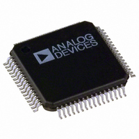
ADE7566ASTZF8 Analog Devices Inc, ADE7566ASTZF8 Datasheet - Page 53

ADE7566ASTZF8
Manufacturer Part Number
ADE7566ASTZF8
Description
IC ENERGY METER MCU 8K 64LQFP
Manufacturer
Analog Devices Inc
Datasheets
1.ADE7169ASTZF16.pdf
(152 pages)
2.ADE7566ASTZF8-RL.pdf
(136 pages)
3.ADE7169ASTZF16.pdf
(144 pages)
Specifications of ADE7566ASTZF8
Applications
Energy Measurement
Core Processor
8052
Program Memory Type
FLASH (8 kB)
Controller Series
ADE75xx
Ram Size
512 x 8
Interface
I²C, SPI, UART
Number Of I /o
20
Voltage - Supply
3.135 V ~ 3.465 V
Operating Temperature
-40°C ~ 85°C
Mounting Type
Surface Mount
Package / Case
64-LQFP
Ic Function
Single Phase Energy Measurement IC
Supply Voltage Range
3.13V To 3.46V, 2.4V To 3.7V
Operating Temperature Range
-40°C To +85°C
Digital Ic Case Style
LQFP
No. Of Pins
64
Lead Free Status / RoHS Status
Lead free / RoHS Compliant
Available stocks
Company
Part Number
Manufacturer
Quantity
Price
Company:
Part Number:
ADE7566ASTZF8
Manufacturer:
Analog Devices Inc
Quantity:
10 000
Company:
Part Number:
ADE7566ASTZF8-RL
Manufacturer:
Analog Devices Inc
Quantity:
10 000
Voltage Channel ADC
Figure 48 shows the ADC and signal processing chain for the
voltage channel. In waveform sampling mode, the ADC outputs
a signed, twos complement, 24-bit data-word at a maximum
of 25.6 kSPS (MCLK/160). The ADC produces an output code
that is approximately between 0x28F5 (+10,485d) and 0xD70B
(−10,485d).
Channel Sampling
The waveform samples of the current ADC and voltage ADC
can also be routed to the waveform registers to be read by the
MCU core. The active, reactive, and apparent power and energy
calculation remain uninterrupted during waveform sampling.
0.5V, 0.25V,
0.125V, 62.5mV,
31.3mV
V2
0V
V
V
P
N
V2
ANALOG
INPUT
RANGE
PGA2
×1, ×2, ×4,
×8, ×16
{GAIN[7:5]}
0xD70B
0x28F5
0x0000
REFERENCE
Figure 48. ADC and Signal Processing in Voltage Channel
ADC
ADE7116/ADE7156/ADE7166/ADE7169/ADE7566/ADE7569
VOLTAGE CHANNEL
WAVEFORM
DATA RANGE
HPF
Rev. B | Page 53 of 152
ACTIVE AND REACTIVE
POWER CALCULATION
f
–3dB
MODE 1[6]
WAVEFORM SAMPLE
REGISTER
VOLTAGE PEAK DETECT
When in waveform sampling mode, one of four output sample
rates can be chosen by using the DTRT[1:0] bits of the
WAVMODE register (see Table 35). The output sample rate can
be 25.6 kSPS, 12.8 kSPS, 6.4 kSPS, or 3.2 kSPS. If the WFSM
enable bit is set in the Interrupt Enable 3 SFR (MIRQENH,
Address 0xDB), the 8052 core has a pending ADE interrupt.
The sampled signals selected in the WAVMODE register are
latched into the waveform SFRs when the waveform high byte
(WAV1H or WAV2H) is read.
The ADE interrupt stays active until the WFSM status bit is
cleared (see the Energy Measurement Interrupts section).
VOLTAGE RMS (V
CALCULATION
LPF1
= 63.7Hz
rms
0x1DD0
0xDFC9
0xE230
ZX DETECTION
0x0000
0x2037
0x0000
)
ZX SIGNAL
DATA RANGE FOR 50Hz SIGNAL
ZX SIGNAL
DATA RANGE FOR 60Hz SIGNAL


