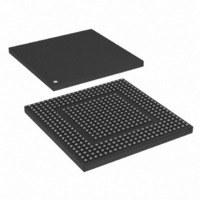
MPC8308VMAGD Freescale Semiconductor, MPC8308VMAGD Datasheet - Page 3

MPC8308VMAGD
Manufacturer Part Number
MPC8308VMAGD
Description
MPU POWERQUICC II PRO 473MAPBGA
Manufacturer
Freescale Semiconductor
Datasheets
1.MPC8308VMAGD.pdf
(90 pages)
2.MPC8308VMAGD.pdf
(2 pages)
3.MPC8308VMAGD.pdf
(1170 pages)
4.MPC8308VMAGD.pdf
(14 pages)
Specifications of MPC8308VMAGD
Processor Type
MPC83xx PowerQUICC II Pro 32-Bit
Speed
400MHz
Voltage
1V
Mounting Type
Surface Mount
Package / Case
473-MAPBGA
Product
Network Processor
Data Rate
256 bps
Frequency
400 MHz
Supply Voltage (max)
3.6 V
Supply Voltage (min)
3 V
Supply Current (max)
5 uA
Maximum Operating Temperature
+ 105 C
Minimum Operating Temperature
0 C
Interface
I2C, JTAG, SPI
Mounting Style
SMD/SMT
Lead Free Status / RoHS Status
Lead free / RoHS Compliant
Features
-
Lead Free Status / Rohs Status
Lead free / RoHS Compliant
Available stocks
Company
Part Number
Manufacturer
Quantity
Price
Company:
Part Number:
MPC8308VMAGD
Manufacturer:
FREESCAL
Quantity:
300
Company:
Part Number:
MPC8308VMAGD
Manufacturer:
Freescale Semiconductor
Quantity:
10 000
Part Number:
MPC8308VMAGD
Manufacturer:
FREESCALE
Quantity:
20 000
Company:
Part Number:
MPC8308VMAGD400/266
Manufacturer:
FREESCAL
Quantity:
300
Company:
Part Number:
MPC8308VMAGDA
Manufacturer:
Freescale Semiconductor
Quantity:
10 000
SERDES PHY
eTSEC I/O Voltage
Input voltage
Storage temperature range
Notes:
1. Functional and tested operating conditions are given in
2. Caution: MV
3. Caution: OV
4. Caution: LV
5. (M, L, O)V
6. The max value of supply voltage should be selected based on the RGMII mode. The lower range applies to RGMII mode.
7. NV
8. LV
2.1.2
Table 2
the recommended and tested operating conditions. Proper device operation outside of these conditions is
not guaranteed.
Freescale Semiconductor
SerDes internal digital power
SerDes internal digital power
SerDes I/O digital power
SerDes analog power for PLL
SerDes analog power for PLL
SerDes I/O digital power
functional operation at the maximums is not guaranteed. Stresses beyond those listed may affect device reliability or cause
permanent damage to the device.
power-on reset and power-down sequences.
power-on reset and power-down sequences.
reset and power-down sequences.
DD1
DD
here refers to NV
here refers to NV
provides the recommended operating conditions for the device. Note that the values in
IN
Power Supply Voltage Specification
IN
and MV
IN
IN
must not exceed LV
DDR2 DRAM signals
DDR2 DRAM reference
eTSEC
Local bus, DUART, system control and power
management, eSDHC, I
Ethernet management, SPI, Miscellaneous
and JTAG I/O voltage
must not exceed NV
must not exceed GV
REF
Characteristic
MPC8308 PowerQUICC II Pro Processor Hardware Specification, Rev. 2
DDA
DDC
Characteristic
may overshoot/undershoot to a voltage and for a maximum duration as shown in
, NV
and LV
DDB
Table 1. Absolute Maximum Ratings
DD
Table 2. Recommended Operating Conditions
,NV
DD2
DD
DD
by more than 0.3 V. This limit may be exceeded for a maximum of 20 ms during power-on
by more than 0.3 V. This limit may be exceeded for a maximum of 20 ms during
2
DDG
by more than 0.3 V. This limit may be exceeded for a maximum of 20 ms during
refers to NV
C, Interrupt,
, NV
DDH
, NV
DDF
Table
DDJ
from the ball map
, NV
2. Absolute maximum ratings are stress ratings only, and
LV
XCOREV
DDP_K
XPADV
SDAV
Symbol
DD1,
MV
MV
T
OV
LV
STG
REF
IN
LV
IN
IN
from the ball map.
XCOREV
XCOREV
DD
DD
XPADV
XPADV
DD2
DD
SDAV
Symbol
SDAV
,
1
,
(continued)
DD
SS
DD
SS
DD
SS
–0.3 to (GV
–0.3 to (GV
–0.3 to (NV
–0.3 to (LV
–0.3 to 2.75 or
–0.3 to 1.26
Max Value
–0.3 to 3.6
–55 to 150
Recommended Value
DD
DD
DD
DD
1.0 V ± 50 mV
1.0 V ± 50 mV
1.0 V ± 50 mV
+ 0.3)
+ 0.3)
+ 0.3)
+ 0.3)
0.0
Electrical Characteristics
0
0
Figure 2
Unit
°C
Table 2
V
V
V
V
V
V
1
Notes
4, 5,8
3, 5,7
Unit
2, 5
2, 5
6,8
V
V
V
V
V
V
—
—
are
3


