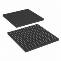
MPC8308VMAGD Freescale Semiconductor, MPC8308VMAGD Datasheet - Page 5

MPC8308VMAGD
Manufacturer Part Number
MPC8308VMAGD
Description
MPU POWERQUICC II PRO 473MAPBGA
Manufacturer
Freescale Semiconductor
Datasheets
1.MPC8308VMAGD.pdf
(90 pages)
2.MPC8308VMAGD.pdf
(2 pages)
3.MPC8308VMAGD.pdf
(1170 pages)
4.MPC8308VMAGD.pdf
(14 pages)
Specifications of MPC8308VMAGD
Processor Type
MPC83xx PowerQUICC II Pro 32-Bit
Speed
400MHz
Voltage
1V
Mounting Type
Surface Mount
Package / Case
473-MAPBGA
Product
Network Processor
Data Rate
256 bps
Frequency
400 MHz
Supply Voltage (max)
3.6 V
Supply Voltage (min)
3 V
Supply Current (max)
5 uA
Maximum Operating Temperature
+ 105 C
Minimum Operating Temperature
0 C
Interface
I2C, JTAG, SPI
Mounting Style
SMD/SMT
Lead Free Status / RoHS Status
Lead free / RoHS Compliant
Features
-
Lead Free Status / Rohs Status
Lead free / RoHS Compliant
Available stocks
Company
Part Number
Manufacturer
Quantity
Price
Company:
Part Number:
MPC8308VMAGD
Manufacturer:
FREESCAL
Quantity:
300
Company:
Part Number:
MPC8308VMAGD
Manufacturer:
Freescale Semiconductor
Quantity:
10 000
Part Number:
MPC8308VMAGD
Manufacturer:
FREESCALE
Quantity:
20 000
Company:
Part Number:
MPC8308VMAGD400/266
Manufacturer:
FREESCAL
Quantity:
300
Company:
Part Number:
MPC8308VMAGDA
Manufacturer:
Freescale Semiconductor
Quantity:
10 000
Figure 2
2.1.3
Table 3
2.1.4
The device does not require the core supply voltage (V
NV
are stable and if the I/O voltages are supplied before the core voltage, there might be a period of time that
all input and output pins are actively driven and cause contention and excessive current. In order to avoid
actively driving the I/O pins and to eliminate excessive current draw, apply the core voltage (V
the I/O voltage (GV
In the case where the core voltage is applied first, the core voltage supply must rise to 90% of its nominal
value before the I/O supplies reach 0.7 V; see
Freescale Semiconductor
DD
1
Local bus interface utilities signals
DDR2 signals
DUART, system control, I
eTSEC signals
) to be applied in any particular order. Note that during power ramp-up, before the power supplies
Output Impedance can also be adjusted through configurable options in DDR Control Driver Register (DDRCDR).
For more information, see the MPC8308 PowerQUICC II Pro Processor Reference Manual .
provides information on the characteristics of the output driver strengths.
shows the undershoot and overshoot voltages at the interfaces of the device.
Output Driver Characteristics
Power Sequencing
V
V
Note:
IH
1. Note that t
IL
1
G/L/NV
G/L/NV
DD
MPC8308 PowerQUICC II Pro Processor Hardware Specification, Rev. 2
Figure 2. Overshoot/Undershoot Voltage for GVDD/NVDD/LVDD
VSS – 0.3 V
VSS – 0.7 V
, LV
G/L/NV
DD
interface
DD
Driver Type
2
C, JTAG, eSDHC, GPIO,SPI, USB
DD
+ 20%
+ 5%
VSS
, and NV
DD
refers to the clock period associated with the bus clock interface.
Table 3. Output Drive Capability
DD
) and assert PORESET before the power supplies fully ramp up.
Figure
Not to Exceed 10%
of t
3.
DD
interface
Output Impedance (Ω)
) and IO supply voltages (GV
1
42
18
42
42
LV
Supply Voltage
NV
GV
NV
DD
Electrical Characteristics
DD
DD
DD
= 2.5/3.3 V
DD
= 3.3 V
= 3.3 V
= 1.8 V
, LV
DD
DD
) before
, and
5


