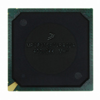
MPC8315ECVRAGDA Freescale Semiconductor, MPC8315ECVRAGDA Datasheet - Page 107

MPC8315ECVRAGDA
Manufacturer Part Number
MPC8315ECVRAGDA
Description
MPU POWERQUICC II PRO 620-PBGA
Manufacturer
Freescale Semiconductor
Datasheet
1.MPC8315VRADDA.pdf
(112 pages)
Specifications of MPC8315ECVRAGDA
Processor Type
MPC83xx PowerQUICC II Pro 32-Bit
Speed
400MHz
Voltage
1V
Mounting Type
Surface Mount
Package / Case
620-PBGA
Processor Series
MPC8xxx
Core
e300
Data Bus Width
32 bit
Maximum Clock Frequency
50 MHz
Maximum Operating Temperature
+ 105 C
Mounting Style
SMD/SMT
Minimum Operating Temperature
- 40 C
Leaded Process Compatible
Yes
Rohs Compliant
Yes
Peak Reflow Compatible (260 C)
Yes
Lead Free Status / RoHS Status
Lead free / RoHS Compliant
Features
-
Lead Free Status / Rohs Status
Lead free / RoHS Compliant
Available stocks
Company
Part Number
Manufacturer
Quantity
Price
Company:
Part Number:
MPC8315ECVRAGDA
Manufacturer:
Freescale Semiconductor
Quantity:
135
Company:
Part Number:
MPC8315ECVRAGDA
Manufacturer:
FREESCAL
Quantity:
36
Company:
Part Number:
MPC8315ECVRAGDA
Manufacturer:
Freescale Semiconductor
Quantity:
10 000
Part Number:
MPC8315ECVRAGDA
Manufacturer:
FREESCALE
Quantity:
20 000
There are a number of ways to reliably provide power to the PLLs, but the recommended solution is to
provide independent filter circuits as illustrated in
independent filters to each PLL the opportunity to cause noise injection from one PLL to the other is
reduced.
This circuit is intended to filter noise in the PLLs resonant frequency range from a 500 kHz to 10 MHz
range. It should be built with surface mount capacitors with minimum Effective Series Inductance (ESL).
Consistent with the recommendations of Dr. Howard Johnson in High Speed Digital Design: A Handbook
of Black Magic (Prentice Hall, 1993), multiple small capacitors of equal value are recommended over a
single large value capacitor.
Each circuit should be placed as close as possible to the specific AV
noise coupled from nearby circuits. It should be possible to route directly from the capacitors to the AV
pin, which is on the periphery of package, without the inductance of vias. Note that the RC filter results in
lower voltage level on AVDD. This does not imply that the DC specification can be relaxed.
Figure 63
26.3
Due to large address and data buses, and high operating frequencies, the device can generate transient
power surges and high frequency noise in its power supply, especially while driving large capacitive loads.
This noise must be prevented from reaching other components in the MPC8315E system, and the
MPC8315E itself requires a clean, tightly regulated source of power. Therefore, it is recommended that
the system designer place at least one decoupling capacitor at each VDD, NVDD, GVDD, and LVDD pins
of the device. These decoupling capacitors should receive their power from separate VDD, NVDD,
GVDD, LVDD, and GND power planes in the PCB, utilizing thick and short traces to minimize
inductance. Capacitors may be placed directly under the device using a standard escape pattern. Others
may surround the part.
These capacitors should have a value of 0.01 or 0.1 µF. Only ceramic SMT (surface mount technology)
capacitors should be used to minimize lead inductance, preferably 0402 or 0603 sizes.
In addition, it is recommended that there be several bulk storage capacitors distributed around the PCB,
feeding the VDD, NVDD, GVDD, and LVDD planes, to enable quick recharging of the smaller chip
capacitors. These bulk capacitors should have a low ESR (equivalent series resistance) rating to ensure the
quick response time necessary. They should also be connected to the power and ground planes through two
vias to minimize inductance. Suggested bulk capacitors—100–330 µF (AVX TPS tantalum or Sanyo
OSCON).
Freescale Semiconductor
Decoupling Recommendations
shows the PLL power supply filter circuit.
MPC8315E PowerQUICC
VDD
Figure 63. PLL Power Supply Filter Circuit
10 Ω
™
2.2 µF
II Pro Processor Hardware Specifications, Rev. 0
GND
Figure
Low ESL Surface Mount Capacitors
2.2 µF
63, one to each of the AV
DD
AV
DD
pin being supplied to minimize
(or L2AV
DD
DD
)
System Design Information
pins. By providing
DD
107


