MPC8315ECVRAGDA Freescale Semiconductor, MPC8315ECVRAGDA Datasheet - Page 13
MPC8315ECVRAGDA
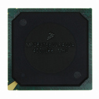
Manufacturer Part Number
MPC8315ECVRAGDA
Description
MPU POWERQUICC II PRO 620-PBGA
Manufacturer
Freescale Semiconductor
Datasheet
1.MPC8315VRADDA.pdf
(112 pages)
Specifications of MPC8315ECVRAGDA
Processor Type
MPC83xx PowerQUICC II Pro 32-Bit
Speed
400MHz
Voltage
1V
Mounting Type
Surface Mount
Package / Case
620-PBGA
Processor Series
MPC8xxx
Core
e300
Data Bus Width
32 bit
Maximum Clock Frequency
50 MHz
Maximum Operating Temperature
+ 105 C
Mounting Style
SMD/SMT
Minimum Operating Temperature
- 40 C
Leaded Process Compatible
Yes
Rohs Compliant
Yes
Peak Reflow Compatible (260 C)
Yes
Lead Free Status / RoHS Status
Lead free / RoHS Compliant
Features
-
Lead Free Status / Rohs Status
Lead free / RoHS Compliant
Available stocks
Company
Part Number
Manufacturer
Quantity
Price
Company:

Part Number:
MPC8315ECVRAGDA
Manufacturer:
Freescale Semiconductor
Quantity:
135
Company:
Part Number:
MPC8315ECVRAGDA
Manufacturer:
FREESCAL
Quantity:
36
Company:
Part Number:
MPC8315ECVRAGDA
Manufacturer:
Freescale Semiconductor
Quantity:
10 000
Part Number:
MPC8315ECVRAGDA
Manufacturer:
FREESCALE
Quantity:
20 000


When switching from normal mode to D3 warm (standby) mode, first turn off the switchable I/O voltage
supply and then turn off the switchable core voltage supply. Similarly, when switching from D3 warm
(standby) mode to normal mode, first turn on the switchable core voltage supply and then turn on the
switchable I/O voltage supply.
An example of the power-up sequence is shown in
warm mode.
The switchable and continuous supplies can be combined when the D3 warm mode is not used.
The SATA power supplies VDD33PLL and VDD33ANA should go high after NVDD3_OFF supply and
go low before NVDD3_OFF supply. The NVDD3_OFF voltage levels should not drop below the
VDD33PLL, VDD33ANA voltages at any time.
Freescale Semiconductor
90%
V
When the device is in D3 warm (standby) mode, all external voltage
supplies applied to any I/O pins, with the exception of wake-up pins, must
be turned off. Applying supplied external voltage to any I/O pins, except the
wake up pins, while the device is in D3 warm standby mode may cause
permanent damage to the device.
Figure 4. Power Up Sequencing Example with Low power D3 Warm Mode
0
MPC8315E PowerQUICC
PORESET
™
II Pro Processor Hardware Specifications, Rev. 0
(LVDDx_ON, NVDDx_ON)
Continuous I/O Voltage
Continuous Core Voltage
VDDC
CAUTION
Figure 4
when implemented along with low power D3
t
SYS_CLK_IN
(GVDD, LVDDx_OFF, NVDDx_OFF)
Switchable I/O Voltage
/ t
Switchable Core Voltage
(VDD)
PCI_SYNC_IN
>= 32 clock
Electrical Characteristics
t
13
Related parts for MPC8315ECVRAGDA
Image
Part Number
Description
Manufacturer
Datasheet
Request
R

Part Number:
Description:
BOARD MPU 8315 POWERQUICC II
Manufacturer:
Freescale Semiconductor
Datasheet:

Part Number:
Description:
PROCESSOR BOARD PWRQUICCII PBGA
Manufacturer:
Freescale Semiconductor
Datasheet:
Part Number:
Description:
PowerQUICC II Pro Processor Hardware Specifications
Manufacturer:
Freescale Semiconductor

Part Number:
Description:
Manufacturer:
Freescale Semiconductor, Inc
Datasheet:
Part Number:
Description:
Manufacturer:
Freescale Semiconductor, Inc
Datasheet:
Part Number:
Description:
Manufacturer:
Freescale Semiconductor, Inc
Datasheet:
Part Number:
Description:
Manufacturer:
Freescale Semiconductor, Inc
Datasheet:
Part Number:
Description:
Manufacturer:
Freescale Semiconductor, Inc
Datasheet:
Part Number:
Description:
Manufacturer:
Freescale Semiconductor, Inc
Datasheet:
Part Number:
Description:
Manufacturer:
Freescale Semiconductor, Inc
Datasheet:
Part Number:
Description:
Manufacturer:
Freescale Semiconductor, Inc
Datasheet:
Part Number:
Description:
Manufacturer:
Freescale Semiconductor, Inc
Datasheet:
Part Number:
Description:
Manufacturer:
Freescale Semiconductor, Inc
Datasheet:
Part Number:
Description:
Manufacturer:
Freescale Semiconductor, Inc
Datasheet:
Part Number:
Description:
Manufacturer:
Freescale Semiconductor, Inc
Datasheet: