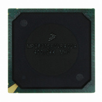
MPC8315ECVRAGDA Freescale Semiconductor, MPC8315ECVRAGDA Datasheet - Page 28

MPC8315ECVRAGDA
Manufacturer Part Number
MPC8315ECVRAGDA
Description
MPU POWERQUICC II PRO 620-PBGA
Manufacturer
Freescale Semiconductor
Datasheet
1.MPC8315VRADDA.pdf
(112 pages)
Specifications of MPC8315ECVRAGDA
Processor Type
MPC83xx PowerQUICC II Pro 32-Bit
Speed
400MHz
Voltage
1V
Mounting Type
Surface Mount
Package / Case
620-PBGA
Processor Series
MPC8xxx
Core
e300
Data Bus Width
32 bit
Maximum Clock Frequency
50 MHz
Maximum Operating Temperature
+ 105 C
Mounting Style
SMD/SMT
Minimum Operating Temperature
- 40 C
Leaded Process Compatible
Yes
Rohs Compliant
Yes
Peak Reflow Compatible (260 C)
Yes
Lead Free Status / RoHS Status
Lead free / RoHS Compliant
Features
-
Lead Free Status / Rohs Status
Lead free / RoHS Compliant
Available stocks
Company
Part Number
Manufacturer
Quantity
Price
Company:
Part Number:
MPC8315ECVRAGDA
Manufacturer:
Freescale Semiconductor
Quantity:
135
Company:
Part Number:
MPC8315ECVRAGDA
Manufacturer:
FREESCAL
Quantity:
36
Company:
Part Number:
MPC8315ECVRAGDA
Manufacturer:
Freescale Semiconductor
Quantity:
10 000
Part Number:
MPC8315ECVRAGDA
Manufacturer:
FREESCALE
Quantity:
20 000
Ethernet: Three-Speed Ethernet, MII Management
Figure 12
9.2.2
This section describes the RMII transmit and receive AC timing specifications.
9.2.2.1
This section describes the RMII transmit and receive AC timing specifications.
RMII transmit AC timing specifications.
28
At recommended operating conditions with LVDD of 3.3 V ± 300 mv
REF_CLK clock
REF_CLK duty cycle
REF_CLK to RMII data TXD[1:0], TX_EN delay
REF_CLK data clock rise V
REF_CLK data clock fall V
Note:
1. The symbols used for timing specifications herein follow the pattern of t
(reference)(state)
symbolizes RMII transmit timing (RMT) for the time t
(X). Note that, in general, the clock reference symbol representation is based on two to three letters representing the clock
of a particular functional. For example, the subscript of t
times, the latter convention is used with the appropriate letter: R (rise) or F (fall).
shows the MII receive AC timing diagram.
RMII AC Timing Specifications
RMII Transmit AC Timing Specifications
for inputs and t
RXD[3:0]
RX_CLK
Parameter/Condition
Figure 12. MII Receive AC Timing Diagram RMII AC Timing Specifications
RX_DV
RX_ER
MPC8315E PowerQUICC
IH
IL
(max) to V
(min) to V
(first two letters of functional block)(reference)(state)(signal)(state)
Table 27. RMII Transmit AC Timing Specifications
t
t
IH
IL
MRXH
MRDVKH
(min)
(max)
t
MRX
™
II Pro Processor Hardware Specifications, Rev. 0
RMX
Valid Data
RMX
clock reference (K) going high (H) until data outputs (D) are invalid
represents the RMII(RM) reference (X) clock. For rise and fall
t
t
RMXH/
Symbol
t
MRXF
RMTKHDX
t
t
t
RMXR
RMXF
RMX
t
RMX
1
(first three letters of functional block)(signal)(state)
t
MRDXKH
t
MRXR
Min
1.0
1.0
35
—
2
for outputs. For example, t
Typ
20
—
—
—
—
Table 27
Freescale Semiconductor
provides the
Max
4.0
4.0
65
10
—
RMTKHDX
Unit
ns
ns
ns
ns
%


