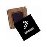
MPC8255ACZUMHBB Freescale Semiconductor, MPC8255ACZUMHBB Datasheet - Page 3

MPC8255ACZUMHBB
Manufacturer Part Number
MPC8255ACZUMHBB
Description
IC MPU POWERQUICC II 480-TBGA
Manufacturer
Freescale Semiconductor
Specifications of MPC8255ACZUMHBB
Processor Type
MPC82xx PowerQUICC II 32-bit
Speed
266MHz
Voltage
2V
Mounting Type
Surface Mount
Package / Case
480-TBGA
Family Name
MPC82XX
Device Core
PowerQUICC II
Device Core Size
32b
Frequency (max)
266MHz
Instruction Set Architecture
RISC
Supply Voltage 1 (typ)
2V
Operating Supply Voltage (max)
2.1V
Operating Supply Voltage (min)
1.9V
Operating Temp Range
-40C to 105C
Operating Temperature Classification
Industrial
Mounting
Surface Mount
Pin Count
480
Package Type
TBGA
Lead Free Status / RoHS Status
Contains lead / RoHS non-compliant
Features
-
Lead Free Status / Rohs Status
Not Compliant
Available stocks
Company
Part Number
Manufacturer
Quantity
Price
Company:
Part Number:
MPC8255ACZUMHBB
Manufacturer:
MOTOROLA
Quantity:
745
Company:
Part Number:
MPC8255ACZUMHBB
Manufacturer:
Freescale Semiconductor
Quantity:
10 000
Part Number:
MPC8255ACZUMHBB
Manufacturer:
FREESCALE
Quantity:
20 000
•
•
•
•
•
•
•
•
Separate power supply for internal logic (2.5 V in HiP3, 2.0 V in HiP4) and for I/O (3.3V)
Separate PLLs for G2 core and for the CPM
— G2 core and CPM can run at different frequencies for power/performance optimization
— Internal core/bus clock multiplier that provides 1.5:1, 2:1, 2.5:1, 3:1, 3.5:1, 4:1, 5:1, 6:1 ratios
— Internal CPM/bus clock multiplier that provides 2:1, 2.5:1, 3:1, 3.5:1, 4:1, 5:1, 6:1 ratios
64-bit data and 32-bit address 60x bus
— Bus supports multiple master designs
— Supports single- and four-beat burst transfers
— 64-, 32-, 16-, and 8-bit port sizes controlled by on-chip memory controller
— Supports data parity or ECC and address parity
32-bit data and 18-bit address local bus
— Single-master bus, supports external slaves
— Eight-beat burst transfers
— 32-, 16-, and 8-bit port sizes controlled by on-chip memory controller
System interface unit (SIU)
— Clock synthesizer
— Reset controller
— Real-time clock (RTC) register
— Periodic interrupt timer
— Hardware bus monitor and software watchdog timer
— IEEE 1149.1 JTAG test access port
Twelve-bank memory controller
— Glueless interface to SRAM, page mode SDRAM, DRAM, EPROM, Flash and other user-
— Byte write enables and selectable parity generation
— 32-bit address decodes with programmable bank size
— Three user programmable machines, general-purpose chip-select machine, and page-mode
— Byte selects for 64 bus width (60x) and byte selects for 32 bus width (local)
— Dedicated interface logic for SDRAM
CPU core can be disabled and the device can be used in slave mode to an external core
Communications processor module (CPM)
— Embedded 32-bit communications processor (CP) uses a RISC architecture for flexible
— Interfaces to G2 core through on-chip 32-Kbyte dual-port RAM and DMA controller
— Serial DMA channels for receive and transmit on all serial channels
— Parallel I/O registers with open-drain and interrupt capability
— Virtual DMA functionality executing memory-to-memory and memory-to-I/O transfers
definable peripherals
pipeline SDRAM machine
support for communications protocols
PRELIMINARY—SUBJECT TO CHANGE WITHOUT NOTICE
Freescale Semiconductor, Inc.
For More Information On This Product,
MPC8255 Hardware Specifications
Go to: www.freescale.com
Features


