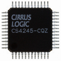
CS4245-CQZ Cirrus Logic Inc, CS4245-CQZ Datasheet - Page 39

CS4245-CQZ
Manufacturer Part Number
CS4245-CQZ
Description
IC CODEC AUD STER 104DB 48LQFP
Manufacturer
Cirrus Logic Inc
Type
Stereo Audior
Datasheet
1.CS4245-CQZ.pdf
(57 pages)
Specifications of CS4245-CQZ
Package / Case
48-LQFP
Data Interface
Serial
Resolution (bits)
24 b
Number Of Adcs / Dacs
2 / 2
Sigma Delta
Yes
Dynamic Range, Adcs / Dacs (db) Typ
104 / 104
Voltage - Supply, Analog
3.13 V ~ 5.25 V
Voltage - Supply, Digital
3.13 V ~ 5.25 V
Operating Temperature
-10°C ~ 70°C
Mounting Type
Surface Mount
Number Of Adc Inputs
12
Number Of Dac Outputs
4
Conversion Rate
192 KSPS
Interface Type
Serial (I2C, SPI)
Resolution
24 bit
Operating Supply Voltage
3.3 V, 5 V
Maximum Operating Temperature
+ 70 C
Mounting Style
SMD/SMT
Minimum Operating Temperature
- 10 C
Number Of Channels
2 ADC/2 DAC
Thd Plus Noise
- 95 dB ADC / - 90 dB DAC
Lead Free Status / RoHS Status
Lead free / RoHS Compliant
For Use With
598-1501 - BOARD EVAL FOR CS4245 CODEC
Lead Free Status / Rohs Status
Lead free / RoHS Compliant
Other names
598-1034
Available stocks
Company
Part Number
Manufacturer
Quantity
Price
Company:
Part Number:
CS4245-CQZ
Manufacturer:
CIRRUS
Quantity:
455
Part Number:
CS4245-CQZ
Manufacturer:
CIRRUS
Quantity:
20 000
Company:
Part Number:
CS4245-CQZR
Manufacturer:
Schneider
Quantity:
1 000
Company:
Part Number:
CS4245-CQZR
Manufacturer:
Cirrus Logic Inc
Quantity:
10 000
DS656F2
4.14
4.15
4.16
Reset
When RESET is low, the CS4245 enters a low-power mode and all internal states are reset, including the
control port and registers, the outputs are muted. When RESET is high, the control port becomes operation-
al, and the desired settings should be loaded into the control registers. Writing a 0 to the PDN bit in the Pow-
er Control register will then cause the part to leave the low-power state and begin operation.
The delta-sigma modulators settle in a matter of microseconds after the analog section is powered, either
through the application of power or by setting the RESET pin high. However, the voltage reference will take
much longer to reach a final value due to the presence of external capacitance on the FILT1+ and FILT2+
pins. During this voltage reference ramp delay, both SDOUT and DAC outputs will be automatically muted.
It is recommended that RESET be activated if the analog or digital supplies drop below the recommended
operating condition to prevent power-glitch-related issues.
Synchronization of Multiple Devices
In systems where multiple ADCs are required, care must be taken to achieve simultaneous sampling. To
ensure synchronous sampling, the master clocks and left/right clocks must be the same for all of the
CS4245s in the system. If only one master clock source is needed, one solution is to place one CS4245 in
Master Mode, and slave all of the other CS4245s to the one master. If multiple master clock sources are
needed, a possible solution would be to supply all clocks from the same external source and time the
CS4245 reset with the inactive edge of master clock. This will ensure that all converters begin sampling on
the same clock edge.
Grounding and Power Supply Decoupling
As with any high-resolution converter, the CS4245 requires careful attention to power supply and grounding
arrangements if its potential performance is to be realized. Figure 12 shows the recommended power ar-
rangements, with VA connected to a clean supply. VD, which powers the digital filter, may be run from the
system logic supply (VLS or VLC) or may be powered from the analog supply (VA) via a resistor. In this
case, no additional devices should be powered from VD. Power supply decoupling capacitors should be as
near to the CS4245 as possible, with the low value ceramic capacitor being the nearest. All signals, espe-
cially clocks, should be kept away from the FILT1+, FILT2+, VQ1 and VQ2 pins in order to avoid unwanted
coupling into the modulators. The FILT1+, FILT2+, VQ1 and VQ2 decoupling capacitors, particularly the
0.1 µF, must be positioned to minimize the electrical path from FILT1+ and FILT2+ and AGND. The CS4245
evaluation board demonstrates the optimum layout and power supply arrangements. To minimize digital
noise, connect the CS4245 digital outputs only to CMOS inputs.
CS4245
39


