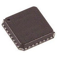
ADAU1381BCPZ Analog Devices Inc, ADAU1381BCPZ Datasheet - Page 25

ADAU1381BCPZ
Manufacturer Part Number
ADAU1381BCPZ
Description
IC AUDIO CODEC STEREO LN 32LFCSP
Manufacturer
Analog Devices Inc
Type
Stereo Audior
Datasheet
1.ADAU1381BCBZ-RL.pdf
(84 pages)
Specifications of ADAU1381BCPZ
Data Interface
Serial, SPI™
Resolution (bits)
24 b
Number Of Adcs / Dacs
2 / 2
Sigma Delta
No
S/n Ratio, Adcs / Dacs (db) Typ
97 / 100
Dynamic Range, Adcs / Dacs (db) Typ
96.5 / 100
Voltage - Supply, Analog
1.8 V ~ 3.65 V
Voltage - Supply, Digital
1.63 V ~ 3.65 V
Operating Temperature
-25°C ~ 85°C
Mounting Type
Surface Mount
Package / Case
32-VFQFN, CSP Exposed Pad
Audio Codec Type
Stereo
No. Of Adcs
2
No. Of Dacs
2
No. Of Input Channels
3
No. Of Output Channels
3
Adc / Dac Resolution
24bit
Adcs / Dacs Signal To Noise Ratio
100dB
Lead Free Status / RoHS Status
Lead free / RoHS Compliant
STARTUP, INITIALIZATION, AND POWER
This section details the procedure for setting up the ADAU1381
properly. Figure 27 provides an overview of how to initialize the IC.
(INCLUDING VOLUME, SAMPLE RATES,
SET UP SOUND ENGINE REGISTERS
SUPPLY POWER TO AVDD1/AVDD2
WAIT 14ms FOR POWER-ON RESET
CONFIGURE CLOCK GENERATION
FOR CUSTOMIZED SIGNAL PATH
AND INITIALIZATION ROM BOOT
AND REGISTER 16386 (0x4002)
AND REGISTER 16513 (0x4081)
ENABLE DIGITAL POWER TO
FUNCTIONAL SUBSYSTEMS
SUPPLY POWER TO IOVDD
SUPPLIED SEPARATELY?
REGISTER 16384 (0x4000)
REGISTER 16512 (0x4080)
ARE AVDD1 AND AVDD2
PINS SIMULTANEOUSLY
FILTER COEFFICIENTS)
WAIT FOR PLL LOCK
(2.4ms TO 3.5ms)
INITIALIZATION
COMPLETE
START
NO
Figure 27. Initialization Sequence
YES
INTERNAL MCLK
(NOT TO SCALE)
CAN AVDD1 AND AVDD2
INPUT/OUTPUT
BE SIMULTANEOUSLY
POWER-UP
(INTERNAL
SUPPLIED?
DVDDOUT
YES
SIGNAL)
AVDD1
AVDD2
IOVDD
PINS
Figure 28. Power-Up and Power-Down Sequence Timing Diagram
HIGH-Z
SUPPLY POWER
SUPPLY POWER
TO AVDD1
TO AVDD2
14ms
NO
Rev. B | Page 25 of 84
1.35V
1.5V
MAIN SUPPLY ENABLED
ACTIVE
POR ACTIVATES
POR COMPLETE/SELF-BOOT INITIATES
SELF-BOOT COMPLETE/MEMORY
IS ACCESSIBLE
1.5V
MAIN SUPPLY DISABLED
POWER-UP SEQUENCE
If AVDD1 and AVDD2 are from the same supply, they can
power up simultaneously. If AVDD1 and AVDD2 are from
separate supplies, then AVDD1 should be powered up first.
IOVDD should be applied simultaneously with AVDD1, if
possible.
The ADAU1381 uses a power-on reset (POR) circuit to reset the
registers upon power-up. The POR monitors the DVDDOUT
pin and generates a reset signal whenever power is applied to
the chip. During the reset, the ADAU1381 is set to the default
values documented in the register map (see the Control Register
Map section).
The POR is also used to prevent clicks and pops on the speaker
driver output. The power-up sequencing and timing involved is
described in Figure 28 in this section, and in Figure 36 and
Figure 37 of the Speaker Output section.
A self-boot ROM initializes the memories after the POR has
completed. When the self-boot sequence is complete, the control
registers are accessible via the I
then be configured as required for the application. Typically,
with a 10 μF capacitor on AVDD1, the power supply ramp-up,
POR, and self-boot combined take approximately 14 ms.
ACTIVE
0.95V
POR
HIGH-Z
2
C/SPI control port and should
ADAU1381


