STLC5046 STMicroelectronics, STLC5046 Datasheet
STLC5046
Specifications of STLC5046
Available stocks


Related parts for STLC5046


STLC5046 Summary of contents
Page 1
... MCU on board. When pin-strap option is selected different pins of the device will change their function (see pin description). In MCU control mode the STLC5046 can be programmed via serial interface running MHz. One interrupt output pin is also provided. ...
Page 2
... Transmit Gain channel #2 (GTX2 Transmit Gain channel #3 (GTX3 Receive Gain channel #0 (GRX0 Receive Gain channel #1 (GRX1 Receive Gain channel #2 (GRX2 Receive Gain channel #3 (GRX3 Transmit Time Slot channel #0 (DXA0 Transmit Time Slot channel#1 (DXA1 Transmit Time Slot channel #2 (DXA2 Doc ID 7052 Rev 5 STLC5046 ...
Page 3
... STLC5046 3.1.18 3.1.19 3.1.20 3.1.21 3.1.22 3.1.23 3.1.24 3.1.25 3.1.26 3.1.27 3.1.28 3.1.29 3.1.30 3.1.31 3.1.32 3.1.33 4 Application circuit . . . . . . . . . . . . . . . . . . . . . . . . . . . . . . . . . . . . . . . . . . 40 5 Electrical characteristics . . . . . . . . . . . . . . . . . . . . . . . . . . . . . . . . . . . . 41 6 Transmission characteristics . . . . . . . . . . . . . . . . . . . . . . . . . . . . . . . . . 46 7 Package information . . . . . . . . . . . . . . . . . . . . . . . . . . . . . . . . . . . . . . . . 49 8 Revision history . . . . . . . . . . . . . . . . . . . . . . . . . . . . . . . . . . . . . . . . . . . 50 Transmit Time Slot channel #3 (DXA3 Receive Time Slot channel #0 (DRA0 Receive Time Slot channel #1 (DRA1) ...
Page 4
... List of tables List of tables Table 1. Device summary . . . . . . . . . . . . . . . . . . . . . . . . . . . . . . . . . . . . . . . . . . . . . . . . . . . . . . . . . . 1 Table 2. I/O definition . . . . . . . . . . . . . . . . . . . . . . . . . . . . . . . . . . . . . . . . . . . . . . . . . . . . . . . . . . . . . 7 Table 3. Pin description . . . . . . . . . . . . . . . . . . . . . . . . . . . . . . . . . . . . . . . . . . . . . . . . . . . . . . . . . . . 7 Table 4. Control byte structure . . . . . . . . . . . . . . . . . . . . . . . . . . . . . . . . . . . . . . . . . . . . . . . . . . . . . 16 Table 5. Registers addresses (only MCU mode Table 6. Electrical characteristics . . . . . . . . . . . . . . . . . . . . . . . . . . . . . . . . . . . . . . . . . . . . . . . . . . . 41 Table 7. Transmission characteristics . . . . . . . . . . . . . . . . . . . . . . . . . . . . . . . . . . . . . . . . . . . . . . . 46 Table 8. Document revision history . . . . . . . . . . . . . . . . . . . . . . . . . . . . . . . . . . . . . . . . . . . . . . . . . 50 4/51 Doc ID 7052 Rev 5 STLC5046 ...
Page 5
... STLC5046 List of figures Figure 1. Block diagram . . . . . . . . . . . . . . . . . . . . . . . . . . . . . . . . . . . . . . . . . . . . . . . . . . . . . . . . . . . . 6 Figure 2. Pin connection (top view Figure 3. Transmit path . . . . . . . . . . . . . . . . . . . . . . . . . . . . . . . . . . . . . . . . . . . . . . . . . . . . . . . . . . . 13 Figure 4. Receive path . . . . . . . . . . . . . . . . . . . . . . . . . . . . . . . . . . . . . . . . . . . . . . . . . . . . . . . . . . . . 13 Figure 5. MCU mode: time slot assignment . . . . . . . . . . . . . . . . . . . . . . . . . . . . . . . . . . . . . . . . . . . . 13 Figure 6. Pin-strap mode: time slot assignment Figure 7. Typical application circuit with STLC3080 without metering pulse injection and I/O pins in dynamic mode ...
Page 6
... SUB 40 CAP 39 VFRO1 38 VFXI1 37 VCC1 36 VCC0 35 VFXI0 34 N.C. 33 VFRO0 D98TL405 STLC5046 FS/FS0 MCLK TSX DX DR IO11 IO10 IO9 IO8 IO7 IO6 / FS3 IO5 / FS2 IO4 / FS1 IO3 / PD3 IO2 / GR3 IO1 / PD2 IO0 / GR2 CS3 / GX3 CS2 / GX2 CS1 / GX1 CS0 / GX0 ...
Page 7
... STLC5046 1.1 Pin description Table 2. I/O definition Type AI Analog input AO Analog output ODO Open drain output DI Digital input DO Digital output DIO Digital input/output DTO Digital tristate output DPS Digital power supply APS Analog power supply Table 3. Pin description N. Name Type Analog Receive analog amplifier output channel 0 ...
Page 8
... IO11 DIO SLIC control I/O pin #11. (see IO7 description). Digital (dual mode) 8/ Pin-strap mode: basic functions selected by proper pin strapping 1 0 MCU mode: device controlled via serial interface 0 0 Reset status 1 1 Not allowed Doc ID 7052 Rev 5 Function Mode select STLC5046 ...
Page 9
... STLC5046 Table 3. Pin description (continued) N. Name Type MCU control mode: FS. Frame Sync. Pulse. A pulse or a square wave waveform with an 8kHz repetition rate is applied to this pin to define the start of the receive and transmit frame. Effective start of the frame can be then shifted clock pulses independently ...
Page 10
... Receive gain programming ch. 1, (see GR2 description). MCU control mode: CI. Control Data Input of Serial Control Bus. Control data is shifted in the device when CS is low and clocked by CCLK. 6 CI/PD0 DI/DI Pin-strap control mode: PD0. Power Down command channel 0. (see PD2 description). 10/51 Function Doc ID 7052 Rev 5 STLC5046 ...
Page 11
... STLC5046 Table 3. Pin description (continued) N. Name Type MCU control mode: CO. Control Data Output of Serial Control Bus. Control data is shifted out the device when CS is low and clocked by CCLK. During the first 8 CCLK pulses the CO pin is 5 CO/GR0 DTO/DI H. I., valid data are shifted out during the following 8 CCLK pulses. ...
Page 12
... GXn control input (in Pin-strap): GXn=1 selects the gain corresponding to GTXn=FFh (0 dB) GXn=0 selects the gain corresponding to GTXn=8Fh (-3.5 dB) Different gain value is obtained through proper voltage divider. A/µ coding Law is selected according to AMU pin level: 12/51 Doc ID 7052 Rev 5 STLC5046 ...
Page 13
... STLC5046 AMU=0 µ Law selected. AMU=1 A Law selected. VFXI input must be AC coupled to the signal source; the voltage swing allowed is 1.0Vpp when the preamplifier gain is set 0dB or 0.66Vpp if the gain is set to 3.52dB (MCU mode only); higher levels must be reduced through proper dividers. ...
Page 14
... RXG. 2.5 PCM interface The STLC5046 dedicate five pins (six in pin-strap mode) to the interface with the PCM highways. MCLK represents the bit clock and is also used by the device as a source for the clock of the internal Sigma Delta converter timings. Four possible frequencies can be used: 1.536/1.544 MHz (24 channels PCM frame) ...
Page 15
... STLC5046 DX represent the transmit PCM interface. It remains in high impedance state except during the assigned time slots during which the PCM data byte is shifted out on the rising edge of MCLK. The four channels can be shifted out in any possible timeslot as defined by the DXA0 to DXA3 registers. If one codec is set in Power Down by software programming the corresponding timeslot is set in High Impedance ...
Page 16
... In pin-strap mode the status of the control pins is entered at power-on reset and refreshed at any Frame Sync. cycle. In MCU mode the control information is written to or read from STLC5046 via the serial four wires control bus: CCLK: Control Clock CS: ...
Page 17
... Though, in general, two bytes of the same instruction take two CS separated cycles, STLC5046 can handle the data transfer in a single 16 CCLK CS cycle, in both the directions. One additional wire provided to the control interface is an open drain interrupt output (INT) that goes low when a change of status is detected on the I/O pins. ...
Page 18
... Persistency Check Time for Input A Persistency Check Time for Input B Interrupt register Alarm register Interrupt Mask for Alarm Loopback register Transmit Preamp. Gain Receive Preamp. Gain (ch1 ch0) Receive Preamp. Gain (ch3 ch2) Silicon Revision Identification Code Doc ID 7052 Rev 5 STLC5046 Description ...
Page 19
... STLC5046 3.1 Registers description 3.1.1 Configuration register (CONF) Addr=00h; Reset Value=3Fh Bit7 Bit6 RES LIN RES=0 Normal operation RES=1 Device reset: I/0n and CSn are all inputs H.I. (equivalent to Hw. reset). LIN µ Law PCM encoding LIN=1 Linear encoding (16 bits), two’s complement. ...
Page 20
... For the I/O pins configured as inputs the corresponding D applied to those pins. Pin-strap value: 0 3.1.4 I/O Data register channel #1 (DATA1) Addr=05h; Reset Value=00h Addr=06h; Reset Value=X0h 20/ Bit5 Bit4 Bit5 Bit4 Doc ID 7052 Rev Bit3 Bit2 Bit1 Bit3 Bit2 Bit1 will be written by the values 11.. STLC5046 0 0 Bit0 11..0 Bit0 ...
Page 21
... STLC5046 If bit 4 of CONF register (STA)=0 Dynamic I/O mode: Bit7 Bit6 When CS1 is active D outputs (see DIR register). For the I/O pins configured as inputs the corresponding D be written by the values applied to those pins while CS1 is low. If bit 4 of CONF register (STA)=1 ...
Page 22
... If bit4 of CONF register (STA)=1 Static I/O mode: can be used as general purpose R/W registers, without any direct action on the control of the device. Pin-strap value: 0 22/51 Bit5 Bit4 Bit5 Bit4 Doc ID 7052 Rev 5 Bit3 Bit2 Bit1 will be written 3.. Bit3 Bit2 Bit1 STLC5046 Bit0 Bit0 ...
Page 23
... STLC5046 3.1.7 Transmit Gain channel #0 (GTX0) Addr=0Bh; Reset Value=00h Bit7 Bit6 00h:Stop any transmit signal, null level is transmitted in the corresponding timeslot on DX output. >00h:Digital gain is inserted in the TX path equal to: Pin-strap values: GX0= gain (value = FFh): 1 GX0=0: -3.5 dB gain (value = 8Fh): 1 3.1.8 Transmit Gain channel #1 (GTX1) Addr=0Ch ...
Page 24
... DX output. >00h:Digital gain is inserted in the TX path equal to: Pin-strap values: GX0= gain (value = FFh): 1 24/ Bit5 Bit4 20log[0.25+0.75*(progr. value/256 Bit5 Bit4 20log[0.25+0.75*(progr. value/256 Doc ID 7052 Rev Bit3 Bit2 Bit1 Bit3 Bit2 Bit1 STLC5046 1 Bit0 1 1 Bit0 1 ...
Page 25
... STLC5046 GX0=0: -3.5 dB gain (value = 8Fh): 1 3.1.11 Receive Gain channel #0 (GRX0) Addr=0Fh; Reset Value=00h Bit7 Bit6 00h:Stop any received signal, AGND level is forced on the VFRO0 analog output. >00h:Digital gain is inserted in the RX path equal to: Pin-strap values: GR0=1: -0.8 dB gain (value = E2h): 1 GR0=0: -2.36 dB gain (value = AFh): ...
Page 26
... GR2=1: -0.8 dB gain (value = E2h): 1 GR2=0: -2.36 dB gain (value = AFh): 1 Overall gain including also RXG: GR2 = 1:-0.8 dB; GR2 = 0: -4.3 dB 3.1.14 Receive Gain channel #3 (GRX3) Addr=12h; Reset Value=00h 26/ Bit5 Bit4 20log[0.25+0.75*(progr. value/256 Doc ID 7052 Rev Bit3 Bit2 Bit1 STLC5046 0 1 Bit0 0 1 ...
Page 27
... STLC5046 Bit7 Bit6 00h:Stop any received signal, AGND level is forced on the VFRO3 analog output. >00h:Digital gain is inserted in the TX path equal to: Pin-strap values: GR3=1: -0.8 dB gain (value = E2h): 1 GR3=0: -4.3 dB gain (value = AFh): 1 Overall gain including also RXG: GR3 = 1:-0.8 dB; GR3 = 0: -4 ...
Page 28
... Registers addresses Pin-strap value (value 80h Referred to FS0. 28/ Doc ID 7052 Rev 5 STLC5046 ...
Page 29
... STLC5046 3.1.16 Transmit Time Slot channel#1 (DXA1) Addr=14h; Reset Value=00h Bit7 Bit6 EN1 T16 EN1=0: Selected transmit time slot on DX output is in H.I. EN1=1: Selected transmit time slot on DX output is active carrying out the PCM encoded signal of VFXI1. T16..0:Define time slot number (0 to 127) on which PCM encoded signal of VFXI1 is carried out ...
Page 30
... Example: if T36..T30=00 Pin-strap value (value 80h Referred to FS3. 30/51 TS0 Bit5 Bit4 T35 T34 TS0 Doc ID 7052 Rev 5 TS1 Bit3 Bit2 Bit1 T33 T32 T31 TS1 STLC5046 Bit0 T30 ...
Page 31
... STLC5046 3.1.19 Receive Time Slot channel #0 (DRA0) Addr=17h; Reset Value=00h Bit7 Bit6 EN0 R06 EN0=0: Disable reception of selected time slot. EN0=1: Selected receive time slot on DR input is PCM decoded and transferred to VFRO0 output. R06..0:Define receive time slot number (0 to 127) on carrying the PCM signal to be decoded and transferred to VFRO0 output ...
Page 32
... Receive Time Slot channel #3 (DRA3) Addr=1Ah; Reset Value=00h Bit7 Bit6 EN0 R36 32/51 TS0 Bit5 Bit4 R25 R24 TS0 Bit5 Bit4 R35 R34 Doc ID 7052 Rev 5 TS1 Bit3 Bit2 Bit1 R23 R22 R21 TS1 Bit3 Bit2 Bit1 R33 R32 R31 STLC5046 Bit0 R20 Bit0 R30 ...
Page 33
... STLC5046 EN3=0: Disable reception of selected time slot. EN3=1: Selected receive time slot on DR input is PCM decoded and transferred to VFRO1 output. R36..0:Define receive time slot number (0 to 127) on carrying the PCM signal to be decoded and transferred to VFRO2 output.If linear mode is selected (LIN=1 of CONF register) the 16 bits will be used as linear code as follows: the 8most significative bits in the programmed time slot, the 8 least significative bits in the following timeslot ...
Page 34
... Lines without persistency check generate an immediate interrupt request. Mask register has no effect on those pins configured as outputs, those pins will not generate interrupt. 34/51 MD5 MD4 MD3 MD11 Bit5 Bit4 Bit3 MC3 Doc ID 7052 Rev 5 STLC5046 MD2 MD1 MD0 MD10 MD9 MD8 Bit2 Bit1 Bit0 MC2 ...
Page 35
... STLC5046 Pin-strap value (value=00h 3.1.26 Persistency Check register (PCHK-A/B) Two input signals per channel, labeled A and B, are submitted to persistency check. In dynamic mode (STA=0), A and B inputs of the four channels, are sampled on the multiplexed lines IO0 (pin13) and IO1 (pin14). In static mode (STA=1) the persistency check is performed on four pairs of lines, assigned to ...
Page 36
... POR= Power On Reset is detected during operation. The register ALARM is cleared after reading operation only if signals are inactive. Pin-strap value (value=00h): 36/ Bit5 Bit4 Bit3 ICKF ID3 0 0 Bit5 Bit4 Bit3 Doc ID 7052 Rev 5 STLC5046 Bit2 Bit1 Bit0 ID2 ID1 ID0 Bit2 Bit1 Bit0 POR CKF ...
Page 37
... STLC5046 3.1.29 Interrupt Mask register for Alarm (AMASK) Addr=23h; Reset Value=11b Bit7 Bit6 MCF=1: The corresponding alarm bit (CKF) doesn’t generate interrupt. MCF=0: The corresponding alarm bit (CKF) generates interrupt. Pin-strap value (value=00h): 3.1.30 Loopback register (LOOPB) Addr=24h; Reset Value=00h ...
Page 38
... XG3..0=0: Transmit preamplifier gain ch. 3..0 = 0dB XG3..0=1: Transmit preamplifier gain ch. 3..0 = 3.52dB Overall transmit gain depends on combination of TXG and GTXn registers. For XGn=0 and GTXn=FF 0dBm0 at DX output correspond to -15dBm|600. (137mVrms) at VFXI input. Pin-strap value (value=00h): 38/51 0 Doc ID 7052 Rev 5 STLC5046 ...
Page 39
... STLC5046 3.1.32 Receive Amplifier Gain registers (RXG-10/32) Addr: 26h; Reset Value=00h Addr: 27h; Reset Value=00h BIT7 BIT6 Rn2 Overall receive gain depends on the receive amplifier gain (Rn2..0 setting in RXG reg.) and digital gain (GRXn reg. setting reference: when Rn2..0 is set for 0dB gain and GRXn=FFh (max. gain) 0dBm0 at DR input correspond to a level at VFRO output equal to 547mVrms (e ...
Page 40
... Application circuit 4 Application circuit Figure 7. Typical application circuit with STLC3080 without metering pulse injection and I/O pins in dynamic mode 40/51 Doc ID 7052 Rev 5 STLC5046 ...
Page 41
... STLC5046 5 Electrical characteristics (Typical value 25°C and nominal supply voltage. Minimum and maximum value are guaranteed over the temperature 0 to 70°C range by production testing and supply voltage range shown in the Operating Ranges. Performances over -40 to +85°C are guaranteed by product characterization unless otherwise specified.) Table 6 ...
Page 42
... SCS high 42/51 Test Condition Pull up resistor = 1 kΩ load invalid R Pull up resistor = 1 kΩ load Measured from Measured from Measured from Measured from Pull up resistor = 1 kΩ load Doc ID 7052 Rev 5 STLC5046 Min. Typ. Max 4.096 100 100 Unit ns ns ...
Page 43
... STLC5046 Table 6. Electrical characteristics (continued) Symbol Parameter SLIC control interface timing TCS Chip select repetition rate t Chip select pulse width csw t Time CS low to data input valid DIV t Time data input invalid to CS high DII Time data output available DOA low Time CS high to data output not ...
Page 44
... SSC t HCS CS- BYTE 44/ WFH SDM t HMD SDM t HMD HCS t t SCS SCS t HCS HCD DSD t SDC Doc ID 7052 Rev 5 t WMH WML t DMZ D98TL387C t WMH WML t DMZ D98TL388C t WCH WCL HSC BYTE 2 t DCD t DDZ D99TL454 STLC5046 17 t DZC 17 t DZC ...
Page 45
... STLC5046 Figure 12. SLIC control port timing t t DIV DII t t DOA DON CS1 CS2 CS3 CS4 IO OUT (OUT) CH0 IO IN CH0 (IN) 31.25μs (32KHz) OUT OUT OUT CH1 CH2 CH3 CH1 CH2 CH3 Doc ID 7052 Rev 5 Electrical characteristics OUT OUT CH0 ...
Page 46
... GSX = 3 to -40 dBm0 -0.2 GSX = -40 to -50 dBm0 -0.4 GSX = -50 to -55 dBm0 -1.2 VFXI = +3 dBm0 33 VFXI = 0 to -30 dBm0 36 VFXI = -40 dBm0 30 VFXI = -45 dBm0 25 VFXI = -50 to -55 dBm0 15 Doc ID 7052 Rev 5 STLC5046 Typ. Max. Unit 137 mVrms 0.15 dB +0.15 dB -20 - 0.15 0 -14.0 -32.0 0. ...
Page 47
... STLC5046 Table 7. Transmission characteristics (continued) Symbol Parameter Differential envelope delay (1 (1) DDX to 2.56 kHz input sinewave @ 0dBm0) Absolute delay @ 1 kHz 500 to (1) DAX 2800Hz Single frequency distortion DPXM (µ Law 0 dBm0 sinewave @ 1004 Hz) Single frequency distortion DPXA (A Law 0 dBm0 sinewave @ 820 Hz) ...
Page 48
... DR inputs receive idle signal. Output is measured the 3 idle channels. Input 200 to 3450Hz at 0dBm0 one channel; all other DR inputs and all VFXI inputs receive idle signal. Output is measured at VFRO of the 3 idle channels. Doc ID 7052 Rev 5 STLC5046 Typ. Max. Unit dBrnCo -85 -79 dBm0p 25 ...
Page 49
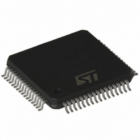
... STLC5046 7 Package information In order to meet environmental requirements, ST offers these devices in different grades of ® ECOPACK packages, depending on their level of environmental compliance. ECOPACK specifications, grade definitions and product status are available at: www.st.com. ® ECOPACK trademark. Figure 13. LQFP64 ( 1.4 mm) mechanical data and package dimensions DIM ...
Page 50
... Revision history 8 Revision history Table 8. Document revision history Date 14-Jan-2004 22-May-2006 20-Aug-2009 50/51 Revision 3 Initial release in EDOCS dms. Added new part number “E-STLC5046”. 4 Changed look and fill. 5 Updated Section 7: Package information on page 49 Doc ID 7052 Rev 5 STLC5046 Changes ...
Page 51
... STLC5046 Information in this document is provided solely in connection with ST products. STMicroelectronics NV and its subsidiaries (“ST”) reserve the right to make changes, corrections, modifications or improvements, to this document, and the products and services described herein at any time, without notice. All ST products are sold pursuant to ST’s terms and conditions of sale. ...