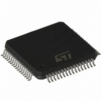
STLC5046 STMicroelectronics, STLC5046 Datasheet - Page 16

STLC5046
Manufacturer Part Number
STLC5046
Description
IC CODEC/FLTR PROG QUAD 64-TQFP
Manufacturer
STMicroelectronics
Type
PCM Codec/Filterr
Specifications of STLC5046
Data Interface
PCM Audio Interface
Resolution (bits)
16 b
Number Of Adcs / Dacs
4 / 4
Sigma Delta
Yes
Voltage - Supply, Analog
3.3 V ~ 5 V
Voltage - Supply, Digital
3.3 V ~ 5 V
Operating Temperature
-40°C ~ 85°C
Mounting Type
Surface Mount
Package / Case
64-TQFP, 64-VQFP
Lead Free Status / RoHS Status
Contains lead / RoHS non-compliant
Other names
497-3665
Available stocks
Company
Part Number
Manufacturer
Quantity
Price
Company:
Part Number:
STLC5046
Manufacturer:
ST
Quantity:
2 282
Part Number:
STLC5046
Manufacturer:
ST
Quantity:
20 000
Company:
Part Number:
STLC5046BCL
Manufacturer:
TOSHIBA
Quantity:
800
Company:
Part Number:
STLC5046BCP
Manufacturer:
ST
Quantity:
1 900
Functional description
2.6
16/51
Finally by means of the LOOPB register is possible to implement a digital or analog
loop_back on any of the selected channels.
TSX represent the Transmit Time Slot (open drain output, 3.2mA). Normally it is floating in
high impedance state except when a time slot is active on the DX output. In this case TSX
output pulls low to enable the backplane line driver. Should be strapped to VSS when not
used.
Table 4.
R/W = 0: Write register
R/W = 1: Read register
D/S = 0: Single byte
D/S = 1: Two bytes
A5..A0: Register Address
Control interface
STLC5046 has two control modes, a microprocessor control mode and a pin-strap control
mode. The two modes are selected by M0 and M1 pins. When M0 = low, M1 = high (MCU
control mode) the MCU port is activated; and the 41 registers of the device can be
programmed. When M0 = high, M1 = low (Pin-strap mode) the microprocessor control port
is disabled and some of the digital pins change their function allowing to perform a very
basic programming of the device.
In pin-strap mode the status of the control pins is entered at power-on reset and refreshed at
any Frame Sync. cycle.
In MCU mode the control information is written to or read from STLC5046 via the serial four
wires control bus:
CCLK: Control Clock
CS:
CI:
CO:
All control instructions require 2 bytes, with the exception of the single byte for command
synchronization. The first byte specify the register address, and the type of access (Read or
Write). The second byte contain the data to be loaded into the register (on CI wire) or
carried out the register content (on CO wire) depending on the R/W bit of the first byte. CO
wire is normally in High Impedance and goes to low impedance only during the second byte
in case of Read operation. This allows to use a common wire for both CI/CO.
Serial data CI is shifted to the serial input register on the rising edge of CCLK and CO is
shifted out on the falling.
R/W
D7
7
Chip Select input
Serial Data input
Serial Data output
Control byte structure
D/S
D6
6
A5
D5
5
Doc ID 7052 Rev 5
First byte (address)
D4
A4
4
A3
D3
3
D2
A2
2
A1
D1
1
STLC5046
A0
D0
0


