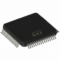
STLC5046 STMicroelectronics, STLC5046 Datasheet - Page 15

STLC5046
Manufacturer Part Number
STLC5046
Description
IC CODEC/FLTR PROG QUAD 64-TQFP
Manufacturer
STMicroelectronics
Type
PCM Codec/Filterr
Specifications of STLC5046
Data Interface
PCM Audio Interface
Resolution (bits)
16 b
Number Of Adcs / Dacs
4 / 4
Sigma Delta
Yes
Voltage - Supply, Analog
3.3 V ~ 5 V
Voltage - Supply, Digital
3.3 V ~ 5 V
Operating Temperature
-40°C ~ 85°C
Mounting Type
Surface Mount
Package / Case
64-TQFP, 64-VQFP
Lead Free Status / RoHS Status
Contains lead / RoHS non-compliant
Other names
497-3665
Available stocks
Company
Part Number
Manufacturer
Quantity
Price
Company:
Part Number:
STLC5046
Manufacturer:
ST
Quantity:
2 282
Part Number:
STLC5046
Manufacturer:
ST
Quantity:
20 000
Company:
Part Number:
STLC5046BCL
Manufacturer:
TOSHIBA
Quantity:
800
Company:
Part Number:
STLC5046BCP
Manufacturer:
ST
Quantity:
1 900
STLC5046
2.5.2
DX represent the transmit PCM interface. It remains in high impedance state except during
the assigned time slots during which the PCM data byte is shifted out on the rising edge of
MCLK.
The four channels can be shifted out in any possible timeslot as defined by the DXA0 to
DXA3 registers. If one codec is set in Power Down by software programming the
corresponding timeslot is set in High Impedance. When linear coding mode is selected by
CONF register programming the output channel will need two consecutive timeslots (see
register description).
DR represent the receive PCM interface. It remains inactive except during the assigned time
slots during which the PCM data byte is shifted in on the falling edge of MCLK. The four
channels are shifted in any possible timeslot as defined by the DRA0 to DRA3 registers.
Figure 6.
Pin-strap mode
When pin-strap mode is selected, dedicated Frame Sync. FS3..0 are provided on dual
function pins:
The PCMSH register cannot be accessed, therefore the beginning of the transmit and
receive frame is identified by the rising edge of the FSn signal.
Each channel has its dedicated Frame Sync. signal FSn. Short or Long frame timing is
automatically selected; depending on the FS signal applied to FS0 input. The assigned
Time Slot (Transmit and Receive) takes place in the 8 MCLK cycles following the falling
edge of FSn in case of Short Frame or the rising edge in case of Long Frame. If one codec
is set in Power Down by proper pin-strap configuration the corresponding timeslot is not
loaded and the VFRO output is kept at steady AGND level.
FS0
D7...................D0
CH0
Pin-strap mode: time slot assignment
MCU
IO4
IO5
IO6
FS
FSn
D7..................D0
Receive /Transmit
Time Slot
CHn
Doc ID 7052 Rev 5
Pin-strap
FS0
FS1
FS2
FS3
FSm
D7...................D0
CHm
Functional description
Pin
14
23
24
62
TS23/31/61/127
15/51


