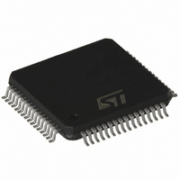
STLC5046 STMicroelectronics, STLC5046 Datasheet - Page 10

STLC5046
Manufacturer Part Number
STLC5046
Description
IC CODEC/FLTR PROG QUAD 64-TQFP
Manufacturer
STMicroelectronics
Type
PCM Codec/Filterr
Specifications of STLC5046
Data Interface
PCM Audio Interface
Resolution (bits)
16 b
Number Of Adcs / Dacs
4 / 4
Sigma Delta
Yes
Voltage - Supply, Analog
3.3 V ~ 5 V
Voltage - Supply, Digital
3.3 V ~ 5 V
Operating Temperature
-40°C ~ 85°C
Mounting Type
Surface Mount
Package / Case
64-TQFP, 64-VQFP
Lead Free Status / RoHS Status
Contains lead / RoHS non-compliant
Other names
497-3665
Available stocks
Company
Part Number
Manufacturer
Quantity
Price
Company:
Part Number:
STLC5046
Manufacturer:
ST
Quantity:
2 282
Part Number:
STLC5046
Manufacturer:
ST
Quantity:
20 000
Company:
Part Number:
STLC5046BCL
Manufacturer:
TOSHIBA
Quantity:
800
Company:
Part Number:
STLC5046BCP
Manufacturer:
ST
Quantity:
1 900
Block diagram and pin connection
Table 3.
10/51
62
28
29
53
52
N.
4
7
6
CCLK/GR1
CS0/GX0
CS1/GX1
CS2/GX2
CS3/GX3
IO6/FS3
CS/PD1
CI/PD0
Name
Pin description (continued)
DIO/DI
DO/DI
DO/DI
DO/DI
DO/DI
Type
DI/DI
DI/DI
DI/DI
MCU control mode: IO4.
Slic control I/O pin #6. (see IO0 description).
Pin-strap control mode: FS3.
Frame sync. pulse of channel #1. One MCLK cycle long, starts PCM data transfer in
the time slot following its falling edge (short frame delayed timing).
MCU control mode: CS0.
Slic CS control #0.
Depending on CONF reg. content can be a CS output for SLIC #0 or a static I/O.
When configured as CS output it is automatically generated by the Codec with a
repetition time of 31.25 µs. In this mode also the IO11.0 are synchronized and carry
proper data in and out synchronous with CS.
Pin-strap control mode: GX0.
Transmit gain programming channel 0:
1: Transmit gain = 0 dB
0: Transmit gain = - 3.5 dB
MCU control mode: CS1:
Slic CS control #1, (see CS0 description).
Pin-strap control mode: GX1.
Transmit gain programming channel 1 (see GX0 description)
MCU control mode: CS2.
Slic CS control #2, (see CS0 description).
Pin-strap control mode: GX2.
Transmit gain programming channel 2 (see GX0 description)
MCU control mode: CS3.
Slic CS control #3, (see CS0 description).
Pin-strap control mode: GX3.
Transmit gain programming channel 3 (see GX0 description)
MCU control mode: CS.
Chip Select of Serial Control Bus. When this pin is low control information can be
written to or read from the device via the CI and CO pins.
Pin-strap control mode: PD1.
Power Down command channel 1. (see PD2 description).
MCU control mode: CCLK.
Clock of Serial Control Bus. This clock shifts serial control information into or out of
CI or CO when CS input is low depending on the current instruction. CCLK may be
asynchronous with the other system clocks.
Pin-strap control mode: GR1.
Receive gain programming ch. 1, (see GR2 description).
MCU control mode: CI.
Control Data Input of Serial Control Bus. Control data is shifted in the device when
CS is low and clocked by CCLK.
Pin-strap control mode: PD0.
Power Down command channel 0. (see PD2 description).
Doc ID 7052 Rev 5
Function
STLC5046


