STLC5048TR STMicroelectronics, STLC5048TR Datasheet - Page 12
STLC5048TR
Manufacturer Part Number
STLC5048TR
Description
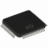
IC CODEC/FILTER PROGR 4CH 64TQFP
Manufacturer
STMicroelectronics
Type
PCM Codec/Filterr
Specifications of STLC5048TR
Data Interface
PCM Audio Interface
Resolution (bits)
16 b
Number Of Adcs / Dacs
4 / 4
Sigma Delta
Yes
Voltage - Supply, Analog
3.3 V ~ 5 V
Voltage - Supply, Digital
3.3 V ~ 5 V
Operating Temperature
-40°C ~ 85°C
Mounting Type
Surface Mount
Package / Case
64-TQFP, 64-VQFP
Lead Free Status / RoHS Status
Lead free / RoHS Compliant
Available stocks
Company
Part Number
Manufacturer
Quantity
Price
Company:

Part Number:
STLC5048TR
Manufacturer:
STMicroelectronics
Quantity:
10 000


Pin assignments and descriptions
Table 5.
12/64
No.
13
12
11
10
24
62
61
60
59
58
57
19
20
21
22
23
28
29
53
52
Pin descriptions (continued)
Name
MCLK
TSXA
IO10
IO11
DRA
DXA
CS0
CS1
CS2
CS3
IO5
IO6
IO7
IO8
IO9
IO0
IO1
IO2
IO3
IO4
Type
ODO
DTO
DIO
DIO
DIO
DIO
DIO
DIO
DIO
DIO
DIO
DIO
DIO
DIO
DIO
DIO
DIO
DIO
DI
DI
Master clock input.
Four possible frequencies can be used:
1.536/1.544 MHz; 2.048 MHz; 4.096 MHz; 8.192 MHz.
The device automatically detect the frequency applied.
This signal is also used as bit clock and it is used to shift data into and out of
the DRA/B and DXA/B pins.
Transmit time slot (open drain output, 3.2mA). Normally it is floating in high
impedance state except when a time slot is active on the DXA output. In this
case TSXA output pulls low to enable the backplane line driver.
Transmit PCM interface A. It remains in high impedance state except during the
assigned time slots during which the PCM data byte is shifted out on the rising
edge of MCLK.
Receive PCM interface A. It remains inactive except during the assigned
receive time slots during which the PCM data byte is shifted in on the falling
edge of MCLK.
General control I/O pin #5. Can be programmed as input or output via DIR
register. Depending on content of CONF register can be a static input/output or
a dynamic input/output synchronized with the CSn output signals controlling
the SLICs.
General control I/O pin #6. (see IO5 description).
General control I/O pin #7. (see IO5 description).
General control I/O pin #8. (see IO5 description).
General control I/O pin #9. (see IO5 description).
General control I/O pin #10. (see IO5 description).
General control I/O pin #11. (see IO5 description).
General control I/O pin #0. (see IO5 description).
General control I/O pin #1. (see IO5 description).
General control I/O pin #2. (see IO5 description).
General control I/O pin #3. (see IO5 description).
General control I/O pin #4. (see IO5 description).
SLIC CS control #0. Depending on CONF reg. content can be a CS output for
SLIC #0 or a static I/O.
When configured as CS output it is automatically generated by the CODEC
with a repetition time of 31.25ms. In this mode also the IO0..11 are
synchronized and carry proper data in and out synchronous with CS.
When configured as static I/O, the direction is defined by CSDIR register
content.
SLIC CS control #1, (see CS0 description).
SLIC CS control #2, (see CS0 description).
SLIC CS control #3, (see CS0 description).
Description
STLC5048
Related parts for STLC5048TR
Image
Part Number
Description
Manufacturer
Datasheet
Request
R

Part Number:
Description:
STMicroelectronics [RIPPLE-CARRY BINARY COUNTER/DIVIDERS]
Manufacturer:
STMicroelectronics
Datasheet:
Part Number:
Description:
STMicroelectronics [LIQUID-CRYSTAL DISPLAY DRIVERS]
Manufacturer:
STMicroelectronics
Datasheet:

Part Number:
Description:
BOARD EVAL FOR MEMS SENSORS
Manufacturer:
STMicroelectronics
Datasheet:
Part Number:
Description:
NPN TRANSISTOR POWER MODULE
Manufacturer:
STMicroelectronics
Datasheet:
Part Number:
Description:
TURBOSWITCH ULTRA-FAST HIGH VOLTAGE DIODE
Manufacturer:
STMicroelectronics
Datasheet:
Part Number:
Description:
Manufacturer:
STMicroelectronics
Datasheet:
Part Number:
Description:
DIODE / SCR MODULE
Manufacturer:
STMicroelectronics
Datasheet:
Part Number:
Description:
DIODE / SCR MODULE
Manufacturer:
STMicroelectronics
Datasheet:
Part Number:
Description:
Search -----> STE16N100
Manufacturer:
STMicroelectronics
Datasheet:
Part Number:
Description:
Search ---> STE53NA50
Manufacturer:
STMicroelectronics
Datasheet:
Part Number:
Description:
NPN Transistor Power Module
Manufacturer:
STMicroelectronics
Datasheet:
Part Number:
Description:
DIODE / SCR MODULE
Manufacturer:
STMicroelectronics
Datasheet: