AD9910BSVZ Analog Devices Inc, AD9910BSVZ Datasheet - Page 12
AD9910BSVZ
Manufacturer Part Number
AD9910BSVZ
Description
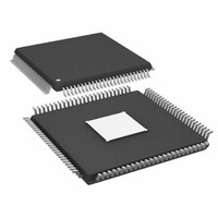
IC DDS 1GSPS 14BIT PAR 100TQFP
Manufacturer
Analog Devices Inc
Datasheet
1.AD9910BSVZ-REEL.pdf
(64 pages)
Specifications of AD9910BSVZ
Design Resources
Synchronizing Multiple AD9910 1 GSPS Direct Digital Synthesizers (CN0121)
Resolution (bits)
14 b
Master Fclk
1GHz
Tuning Word Width (bits)
32 b
Voltage - Supply
1.8V, 3.3V
Operating Temperature
-40°C ~ 85°C
Mounting Type
Surface Mount
Package / Case
100-TQFP Exposed Pad, 100-eTQFP, 100-HTQFP, 100-VQFP
Pll Type
Frequency Synthesis
Frequency
1GHz
Supply Current
29mA
Supply Voltage Range
1.71V To 1.89V
Digital Ic Case Style
TQFP
No. Of Pins
100
Operating Temperature Range
-40°C To +85°C
Lead Free Status / RoHS Status
Lead free / RoHS Compliant
For Use With
AD9910/PCBZ - BOARD EVAL FOR AD9910 1GSPS
Lead Free Status / RoHS Status
Lead free / RoHS Compliant, Lead free / RoHS Compliant
Available stocks
Company
Part Number
Manufacturer
Quantity
Price
Company:

Part Number:
AD9910BSVZ
Manufacturer:
AVAGO
Quantity:
1 400
Company:
Part Number:
AD9910BSVZ
Manufacturer:
ADI
Quantity:
509
Company:
Part Number:
AD9910BSVZ
Manufacturer:
Analog Devices Inc
Quantity:
10 000
Part Number:
AD9910BSVZ
Manufacturer:
ADI/亚德诺
Quantity:
20 000
Company:
Part Number:
AD9910BSVZ-REEL
Manufacturer:
Analog Devices Inc
Quantity:
10 000


AD9910
Pin No.
59
60
61
62
63
67
68
69
70
71
80
81
84
90
91
94
95
96 (EPAD)
1
I = input, O = output.
Mnemonic
I/O_UPDATE
OSK
DROVER
DRCTL
DRHOLD
SDIO
SDO
SCLK
CS
I/O_RESET
IOUT
IOUT
DAC_RSET
REF_CLK
REF_CLK
REFCLK_OUT
XTAL_SEL
Exposed Paddle
(EPAD)
I/O
I/O
I
O
I
I
I/O
O
I
I
I
O
O
O
I
I
O
I
1
Description
Input/Output Update. Digital input (active high). A high on this pin transfers the contents
of the I/O buffers to the corresponding internal registers.
Output Shift Keying. Digital input (active high). When the OSK features are placed in either
manual or automatic mode, this pin controls the OSK function. In manual mode, it toggles
the multiplier between 0 (low) and the programmed amplitude scale factor (high). In
automatic mode, a low sweeps the amplitude down to zero, a high sweeps the amplitude
up to the amplitude scale factor.
Digital Ramp Over. Digital output (active high). This pin switches to Logic 1 whenever the
digital ramp generator reaches its programmed upper or lower limit.
Digital Ramp Control. Digital input (active high). This pin controls the slope polarity of the
digital ramp generator. See the Digital Ramp Generator (DRG) section for more details. If
not using the digital ramp generator, connect this pin to Logic 0.
Digital Ramp Hold. Digital input (active high). This pin stalls the digital ramp generator in
its present state. See the Digital Ramp Generator (DRG) section for more details. If not
using a digital ramp generator, connect this pin to Logic 0.
Serial Data Input/Output. Digital input/output (active high). This pin can be either unidirec-
tional or bidirectional (default), depending on the configuration settings. In bidirectional serial
port mode, this pin acts as the serial data input and output. In unidirectional mode, it is an
input only.
Serial Data Output. Digital output (active high). This pin is only active in unidirectional
serial data mode. In this mode, it functions as the output. In bidirectional mode, this pin is
not operational and should be left floating.
Serial Data Clock. Digital clock (rising edge on write, falling edge on read). This pin provides
the serial data clock for the control data path. Write operations to the AD9910 use the
rising edge. Readback operations from the AD9910 use the falling edge.
Chip Select. Digital input (active low). This pin allows the AD9910 to operate on a common
serial bus for the control data path. Bringing this pin low enables the AD9910 to detect
serial clock rising/falling edges. Bringing this pin high causes the AD9910 to ignore input
on the serial data pins.
Input/Output Reset. Digital input (active high). This pin can be used when a serial I/O
communication cycle fails (see the I/O_RESET—Input/Output Reset section for details).
When not used, connect this pin to ground.
Open-Drain DAC Complementary Output Source. Analog output (current mode). Connect
through a 50 Ω resistor to AGND.
Open-Drain DAC Output Source. Analog output (current mode). Connect through a 50 Ω
resistor to AGND.
Analog Reference Pin. This pin programs the DAC output full-scale reference current.
Attach a 10 kΩ resistor to AGND.
Reference Clock Input. Analog input. When the internal oscillator is engaged, this pin can
be driven by either an external oscillator or connected to a crystal. See the REF_CLK/ Overview
section for more details.
Reference Clock Input. Analog input. See the REF_CLK/ Overview section for more details.
Crystal Output. Analog output. See the REF_CLK/ Overview section for more details.
Crystal Select (1.8 V Logic). Analog input (active high). Driving the XTAL_SEL pin high,
the AVDD (1.8V) pin enables the internal oscillator to be used with a crystal resonator.
If unused, connect it to AGND.
The EPAD should be soldered to ground.
Rev. C | Page 12 of 64
Related parts for AD9910BSVZ
Image
Part Number
Description
Manufacturer
Datasheet
Request
R

Part Number:
Description:
Direct Digital Synthesis Evaluation Board
Manufacturer:
Analog Devices Inc
Datasheet:


Part Number:
Description:
±1.7g Dual-Axis IMEMS Accelerometer Evaluation Board
Manufacturer:
Analog Devices Inc
Datasheet:

Part Number:
Description:
Inertial Sensor Evaluation System
Manufacturer:
Analog Devices Inc
Datasheet:
Part Number:
Description:
Manufacturer:
Analog Devices Inc
Datasheet:
Part Number:
Description:
Manufacturer:
Analog Devices Inc
Datasheet:
Part Number:
Description:
Manufacturer:
Analog Devices Inc
Datasheet:
Part Number:
Description:
Manufacturer:
Analog Devices Inc
Datasheet:
Part Number:
Description:
Manufacturer:
Analog Devices Inc
Datasheet:
Part Number:
Description:
Manufacturer:
Analog Devices Inc
Datasheet:
Part Number:
Description:
Manufacturer:
Analog Devices Inc
Datasheet:
Part Number:
Description:
Manufacturer:
Analog Devices Inc
Datasheet:
Part Number:
Description:
Manufacturer:
Analog Devices Inc
Datasheet: