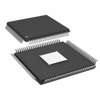
AD9910BSVZ Analog Devices Inc, AD9910BSVZ Datasheet - Page 35

AD9910BSVZ
Manufacturer Part Number
AD9910BSVZ
Description
IC DDS 1GSPS 14BIT PAR 100TQFP
Manufacturer
Analog Devices Inc
Datasheet
1.AD9910BSVZ-REEL.pdf
(64 pages)
Specifications of AD9910BSVZ
Design Resources
Synchronizing Multiple AD9910 1 GSPS Direct Digital Synthesizers (CN0121)
Resolution (bits)
14 b
Master Fclk
1GHz
Tuning Word Width (bits)
32 b
Voltage - Supply
1.8V, 3.3V
Operating Temperature
-40°C ~ 85°C
Mounting Type
Surface Mount
Package / Case
100-TQFP Exposed Pad, 100-eTQFP, 100-HTQFP, 100-VQFP
Pll Type
Frequency Synthesis
Frequency
1GHz
Supply Current
29mA
Supply Voltage Range
1.71V To 1.89V
Digital Ic Case Style
TQFP
No. Of Pins
100
Operating Temperature Range
-40°C To +85°C
Lead Free Status / RoHS Status
Lead free / RoHS Compliant
For Use With
AD9910/PCBZ - BOARD EVAL FOR AD9910 1GSPS
Lead Free Status / RoHS Status
Lead free / RoHS Compliant, Lead free / RoHS Compliant
Available stocks
Company
Part Number
Manufacturer
Quantity
Price
Company:
Part Number:
AD9910BSVZ
Manufacturer:
AVAGO
Quantity:
1 400
Company:
Part Number:
AD9910BSVZ
Manufacturer:
ADI
Quantity:
509
Company:
Part Number:
AD9910BSVZ
Manufacturer:
Analog Devices Inc
Quantity:
10 000
Part Number:
AD9910BSVZ
Manufacturer:
ADI/亚德诺
Quantity:
20 000
Company:
Part Number:
AD9910BSVZ-REEL
Manufacturer:
Analog Devices Inc
Quantity:
10 000
Note that two-level modulation can be accomplished by using
only one of the three profile pins to toggle between two differ-
ent parameter values. Likewise, four-level modulation can be
accomplished by using only two of the three profile pins. There
is no restriction on which profile pins are used.
RAM Direct Switch Mode with Zero Crossing
The zero-crossing function (enabled with the zero-crossing bit)
is a special feature that is only available in RAM direct switch
mode. The zero-crossing function is only valid if the RAM
playback destination bits specify phase as the DDS signal
control parameter.
Enabling zero-crossing causes the DDS to delay the application
of a new phase value until such time as the DDS phase accumula-
tor rolls over from full scale to 0 (the point at which the DDS
phase accumulator represents a phase angle that is at the 360° to
0° transition point). This can be a very beneficial feature when
the DDS is programmed to generate a sine wave (using the
select DDS sine output bit) because the zero-crossing point of
phase for a sine wave corresponds with the zero-crossing point
of amplitude.
In the case of binary phase shift keying (BPSK), the zero-
crossing feature allows the AD9910 to perform the 180° phase
jumps associated with BPSK with only a minimal instantaneous
change in amplitude. This avoids the spectral splatter that
frequently accompanies BPSK modulation.
Although the intent of the zero-crossing feature is for use with
the DDS sine output enabled, it can be used with a cosine
output. In this case, the phase values extracted from RAM are
registered at the DDS when the output amplitude is at its peak
positive value.
RAM Ramp-Up Mode
In ramp-up mode, upon assertion of an I/O update or a change
of profile, the RAM begins operating as a waveform generator
using the parameters programmed into the selected RAM
profile register. Data is extracted from RAM over the specified
address range and at the specified rate contained in the wave-
form start address, waveform end address, and address ramp
rate values of the selected RAM profile. The data is delivered
to the specified DDS signal control parameter(s) based on the
RAM playback destination bits.
The internal state machine begins extracting data from the
RAM at the waveform start address and continues to extract
data until it reaches the waveform end address. Upon reaching
this address, it either remains at the waveform end address or
returns to the waveform start address as defined by the no-dwell
high bit. Then the state machine halts, and the RAM_SWP_OVR
pin goes high.
Rev. C | Page 35 of 64
Ramp-Up Timing Diagram
A graphic representation of the ramp-up mode appears in
Figure 43, showing both normal and no-dwell operation.
The two upper traces show the progression of the RAM address
from the waveform start address to the waveform end address
for the selected profile. The address value advances by one with
each timeout of the timer internal to the state machine. The
timer period (Δt) is determined by the address ramp rate value
for the selected profile. The two upper traces are differentiated
by the state of the no-dwell high bit.
The circled numbers in Figure 43 indicate specific events,
explained as follows:
Event 1—An I/O update or profile change occurs. This event
initializes the state machine to the waveform start address and
sets the RAM_SWP_OVR pin to Logic 0.
Event 2—The state machine reaches the waveform end address
value for the selected profile. The RAM_SWP_OVR pin
switches to Logic 1. This marks the end of the waveform
generation sequence for normal operation.
Event 3—The state machine switches to the waveform start
address. This marks the end of the waveform generation
sequence for no-dwell operation.
Changing profiles resets the RAM_SWP_OVR pin to Logic 0,
automatically terminates the current waveform, and initiates the
newly selected waveform.
RAM_SWP_OVER
RAM ADDRESS
RAM ADDRESS
I/O_UPDATE
Figure 43. Ramp-Up Timing Diagram
WAVEFORM END ADDRESS
1
WAVEFORM START ADDRESS
WAVEFORM START ADDRESS
WAVEFORM END ADDRESS
M DDS CLOCK CYCLES
1
1
Δ
2
t
NO-DWELL
NO-DWELL
3
HIGH = 0
HIGH = 1
AD9910


