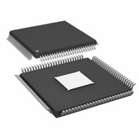
AD9910BSVZ Analog Devices Inc, AD9910BSVZ Datasheet - Page 38

AD9910BSVZ
Manufacturer Part Number
AD9910BSVZ
Description
IC DDS 1GSPS 14BIT PAR 100TQFP
Manufacturer
Analog Devices Inc
Datasheet
1.AD9910BSVZ-REEL.pdf
(64 pages)
Specifications of AD9910BSVZ
Design Resources
Synchronizing Multiple AD9910 1 GSPS Direct Digital Synthesizers (CN0121)
Resolution (bits)
14 b
Master Fclk
1GHz
Tuning Word Width (bits)
32 b
Voltage - Supply
1.8V, 3.3V
Operating Temperature
-40°C ~ 85°C
Mounting Type
Surface Mount
Package / Case
100-TQFP Exposed Pad, 100-eTQFP, 100-HTQFP, 100-VQFP
Pll Type
Frequency Synthesis
Frequency
1GHz
Supply Current
29mA
Supply Voltage Range
1.71V To 1.89V
Digital Ic Case Style
TQFP
No. Of Pins
100
Operating Temperature Range
-40°C To +85°C
Lead Free Status / RoHS Status
Lead free / RoHS Compliant
For Use With
AD9910/PCBZ - BOARD EVAL FOR AD9910 1GSPS
Lead Free Status / RoHS Status
Lead free / RoHS Compliant, Lead free / RoHS Compliant
Available stocks
Company
Part Number
Manufacturer
Quantity
Price
Company:
Part Number:
AD9910BSVZ
Manufacturer:
AVAGO
Quantity:
1 400
Company:
Part Number:
AD9910BSVZ
Manufacturer:
ADI
Quantity:
509
Company:
Part Number:
AD9910BSVZ
Manufacturer:
Analog Devices Inc
Quantity:
10 000
Part Number:
AD9910BSVZ
Manufacturer:
ADI/亚德诺
Quantity:
20 000
Company:
Part Number:
AD9910BSVZ-REEL
Manufacturer:
Analog Devices Inc
Quantity:
10 000
AD9910
Internal Profile Control Continuous Waveform Timing
Diagram
An example of an internal profile control continuous waveform
timing diagram is shown in Figure 45. The diagram assumes that
the internal profile control bits (in Control Function Register 1)
are programmed as 1000. It also assumes that the start address in
RAM Profile 1 is greater than the end address in RAM Profile 0.
The gray bar across the top indicates the time interval over
which the designated profile is in effect. The circled numbers
indicate specific events.
Event 1—An I/O update registers that the internal profile
control bits (in Control Function Register 1) are programmed
to 1000. The RAM_SWP_OVR pin is set to Logic 0. The state
machine is initialized to the waveform start address of RAM
Profile 0 and begins incrementing through the address range for
RAM Profile 0 at intervals of Δt
step rate for RAM Profile 0).
Event 2—The state machine reaches the waveform end address
of RAM Profile 0, and the RAM_SWP_OVR pin generates a
positive pulse spanning two DDS clock cycles.
Event 3—Having reached the waveform end address of RAM
Profile 0, the next expiration of the internal timer causes the
state machine to advance to RAM Profile 1. The state machine
is initialized to the waveform start address of RAM Profile 1
and begins incrementing through the address range for RAM
Profile 1 at intervals of Δt
Event 4—The state machine reaches the waveform end address
of RAM Profile 1, and the RAM_SWP_OVR pin generates a
positive pulse spanning two DDS clock cycles.
Event 5—Having reached the waveform end address of RAM
Profile 1, the next expiration of the internal timer causes the
state machine to jump back to RAM Profile 0. The state
machine initializes to the waveform start address of RAM
RAM_SWP_OVER
I/O_UPDATE
RAM PROFILE
ADDRESS
RAM
1
.
1
Δ
WAVEFORM START
t
WAVEFORM START
0
WAVEFORM END
WAVEFORM END
0
ADDRESS 1
ADDRESS 0
ADDRESS 0
ADDRESS 1
(as specified by the address
0
Figure 45. Internal Profile Control Timing Diagram (Continuous)
1
2
3
Δ
t
1
1
1
Rev. C | Page 38 of 64
4
5
0
Profile 0 and begins incrementing through the address range for
RAM Profile 0 at intervals of Δt
Event 5 to Event 11—These events repeat indefinitely until the
internal profile control bits are reprogrammed and an I/O
update is asserted.
RAM Bidirectional Ramp Mode
In bidirectional ramp mode, upon assertion of an I/O update,
the RAM begins operating as a waveform generator using the
parameters programmed only into RAM Profile 0 (unlike ramp
up mode, which uses all eight profiles). Data is extracted from
RAM over the specified address range and at the specified rate
contained in the waveform start address, waveform end address,
and address ramp rate values of the selected RAM profile. The
data is delivered to the specified DDS signal control parameter(s)
based on the RAM playback destination bits.
The PROFILE[2:1] pins are ignored by the internal logic in this
mode. When a RAM profile programmed to operate in this
mode is selected, no other RAM profiles can be selected until the
active RAM profile is reprogrammed with a different RAM
operating mode. The no-dwell high bit is ignored in this mode.
With the bidirectional ramp mode activated via an I/O update
or profile change, the internal state machine readies to extract
data from the RAM at the waveform start address. Data extrac-
tion begins when PROFILE0 is Logic 1, which instructs the state
machine to begin incrementing through the address range. As
long as the PROFILE0 pin remains Logic 1, the state machine
continues to extract data until it reaches the waveform end
address. At this point, the state machine halts until the PROFILE0
pin is Logic 0, instructing the state machine to begin decrementing
through the address range. As long as the PROFILE0 pin is
Logic 0, the state machine continues to extract data until it
reaches the waveform start address. At this point, the state
machine halts until the PROFILE0 pin is Logic 1.
6
7
1
8
9
0
.
0
10 11
1


