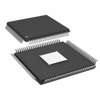
AD9910BSVZ Analog Devices Inc, AD9910BSVZ Datasheet - Page 21

AD9910BSVZ
Manufacturer Part Number
AD9910BSVZ
Description
IC DDS 1GSPS 14BIT PAR 100TQFP
Manufacturer
Analog Devices Inc
Datasheet
1.AD9910BSVZ-REEL.pdf
(64 pages)
Specifications of AD9910BSVZ
Design Resources
Synchronizing Multiple AD9910 1 GSPS Direct Digital Synthesizers (CN0121)
Resolution (bits)
14 b
Master Fclk
1GHz
Tuning Word Width (bits)
32 b
Voltage - Supply
1.8V, 3.3V
Operating Temperature
-40°C ~ 85°C
Mounting Type
Surface Mount
Package / Case
100-TQFP Exposed Pad, 100-eTQFP, 100-HTQFP, 100-VQFP
Pll Type
Frequency Synthesis
Frequency
1GHz
Supply Current
29mA
Supply Voltage Range
1.71V To 1.89V
Digital Ic Case Style
TQFP
No. Of Pins
100
Operating Temperature Range
-40°C To +85°C
Lead Free Status / RoHS Status
Lead free / RoHS Compliant
For Use With
AD9910/PCBZ - BOARD EVAL FOR AD9910 1GSPS
Lead Free Status / RoHS Status
Lead free / RoHS Compliant, Lead free / RoHS Compliant
Available stocks
Company
Part Number
Manufacturer
Quantity
Price
Company:
Part Number:
AD9910BSVZ
Manufacturer:
AVAGO
Quantity:
1 400
Company:
Part Number:
AD9910BSVZ
Manufacturer:
ADI
Quantity:
509
Company:
Part Number:
AD9910BSVZ
Manufacturer:
Analog Devices Inc
Quantity:
10 000
Part Number:
AD9910BSVZ
Manufacturer:
ADI/亚德诺
Quantity:
20 000
Company:
Part Number:
AD9910BSVZ-REEL
Manufacturer:
Analog Devices Inc
Quantity:
10 000
Table 4. Parallel Port Destination Bits
F[1:0]
00
01
10
11
Transmit Enable (TxENABLE)
The AD9910 also accepts a user-generated signal applied to the
TxENABLE pin that acts as a gate for the user-supplied data. By
default, TxENABLE is considered true for Logic 1 and false for
Logic 0. However, the logical behavior of this pin can be reversed
using the TxENABLE invert bit. When TxENABLE is true, the
device latches data into the device on the expected edge of PDCLK
(based on the PDCLK invert bit). When TxENABLE is false,
even though the PDCLK may continue to operate, the device
ignores the data supplied to the port. Furthermore, when the
TxENABLE pin is held false, the device internally clears the
16-bit data-words, or it retains the last value present on the data
port prior to TxENABLE switching to the false state (based on
the setting of the data assembler hold last value bit).
D[15:0]
D[15:2]
D[15:0]
D[15:0]
D[15:8]
D[7:0]
Parameter(s)
14-bit amplitude
parameter (unsigned
integer)
16-bit phase parameter
(unsigned integer)
32-bit frequency
parameter (unsigned
integer)
8-bit amplitude
(unsigned integer)
8-bit phase (unsigned
integer)
Comments
Amplitude scales from 0 to 1 − 2
Phase offset ranges from 0 to 2π(1 − 2
The alignment of the 16-bit data-word with the 32-bit frequency parameter is controlled
by a 4-bit FM gain word in the programming registers.
The MSB of the data-word amplitude aligns with the MSB of the DDS 14-bit amplitude
parameter. The six LSBs of the DDS amplitude parameter are assigned from Bits[5:0] of the
ASF register. The resulting 14-bit word scales the amplitude from 0 to 1 − 2
The MSB of the data-word phase aligns with the MSB of the 16-bit phase parameter of
the DDS. The eight LSBs of the DDS phase parameter are assigned from Bits[7:0] of the
POW register. The resulting 16-bit word offsets the phase from 0 to 2π(1 − 2
Rev. C | Page 21 of 64
Alternatively, instead of operating the TxENABLE pin as a gate,
the user can drive the TxENABLE pin with a clock signal
operating at the parallel port data rate. When driven by a clock
signal, the transition from the false to true state must meet the
required setup and hold time on each cycle to ensure proper
operation. The TxENABLE and PDCLK timing is shown in
Figure 26.
DATA PORT
PARALLEL
TxENABLE
TxENABLE
(CLOCK)
(BURST)
PDCLK
−14
. D[1:0] are not used.
Figure 26. PDCLK and TxENABLE Timing Diagram
t
−16
DS
t
DS
) radians.
WORD 1
TRUE
FALSE
t
DH
WORD 2
WORD 3
WORD 4 WORD N – 4
−14
−16
.
t
DH
) radians.
AD9910
WORD N


