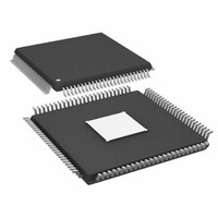
AD9910BSVZ Analog Devices Inc, AD9910BSVZ Datasheet - Page 24

AD9910BSVZ
Manufacturer Part Number
AD9910BSVZ
Description
IC DDS 1GSPS 14BIT PAR 100TQFP
Manufacturer
Analog Devices Inc
Datasheet
1.AD9910BSVZ-REEL.pdf
(64 pages)
Specifications of AD9910BSVZ
Design Resources
Synchronizing Multiple AD9910 1 GSPS Direct Digital Synthesizers (CN0121)
Resolution (bits)
14 b
Master Fclk
1GHz
Tuning Word Width (bits)
32 b
Voltage - Supply
1.8V, 3.3V
Operating Temperature
-40°C ~ 85°C
Mounting Type
Surface Mount
Package / Case
100-TQFP Exposed Pad, 100-eTQFP, 100-HTQFP, 100-VQFP
Pll Type
Frequency Synthesis
Frequency
1GHz
Supply Current
29mA
Supply Voltage Range
1.71V To 1.89V
Digital Ic Case Style
TQFP
No. Of Pins
100
Operating Temperature Range
-40°C To +85°C
Lead Free Status / RoHS Status
Lead free / RoHS Compliant
For Use With
AD9910/PCBZ - BOARD EVAL FOR AD9910 1GSPS
Lead Free Status / RoHS Status
Lead free / RoHS Compliant, Lead free / RoHS Compliant
Available stocks
Company
Part Number
Manufacturer
Quantity
Price
Company:
Part Number:
AD9910BSVZ
Manufacturer:
AVAGO
Quantity:
1 400
Company:
Part Number:
AD9910BSVZ
Manufacturer:
ADI
Quantity:
509
Company:
Part Number:
AD9910BSVZ
Manufacturer:
Analog Devices Inc
Quantity:
10 000
Part Number:
AD9910BSVZ
Manufacturer:
ADI/亚德诺
Quantity:
20 000
Company:
Part Number:
AD9910BSVZ-REEL
Manufacturer:
Analog Devices Inc
Quantity:
10 000
AD9910
Auxiliary DAC
An 8-bit auxiliary DAC controls the full-scale output current of
the main DAC (I
register map location sets I
where R
is the 8-bit value supplied to the auxiliary DAC (default is 127).
For example, with R
20.07 mA.
INVERSE SINC FILTER
The sampled carrier data stream is the input to the digital-to-
analog converter (DAC) integrated into the AD9910. The
DAC output spectrum is shaped by the characteristic sin(x)/x
(or sinc) envelope, due to the intrinsic zero-order hold effect
associated with DAC generated signals. The sinc envelope
can be compensated for because its shape is well known. This
envelope restoration function is provided by the inverse sinc
filter preceding the DAC. The inverse sinc filter is implemented
as a digital FIR filter. It has a response characteristic that very
nearly matches the inverse of the sinc envelope. The response
of the inverse sinc filter is shown in Figure 28 (with the sinc
envelope for comparison).
The inverse sinc filter is enabled using CFR1[22]. The filter tap
coefficients are given in Table 6. The filter operates by distorting
the data prior to its arrival at the DAC in such a way as to
compensate for the sinc envelope that otherwise distorts the
spectrum.
When the inverse sinc filter is enabled, it introduces a ~3.0 dB
insertion loss. The inverse sinc compensation is effective for output
frequencies up to approximately 40% of the DAC sample rate.
Table 6. Inverse Sinc Filter Tap Coefficients
Tap No.
1, 7
2, 6
3, 5
4
In Figure 28, the sinc envelope introduces a frequency dependent
attenuation that can be as much as 4 dB at the Nyquist frequency
(½ of the DAC sample rate). Without the inverse sinc filter, the
DAC output suffers from the frequency dependent droop of
the sinc envelope. The inverse sinc filter effectively flattens the
droop to within ±0.05 dB, as shown in Figure 29, which shows
the corrected sinc response with the inverse sinc filter enabled.
I
OUT
SET
=
is the value of the R
86
R
SET
4 .
OUT
⎛ +
⎜
⎝
1
). An 8-bit code word stored in the appropriate
SET
= 10,000 Ω and CODE = 127, then I
CODE
96
OUT
according to the following equation:
⎞
⎟
⎠
Tap Value
−35
+134
−562
+6729
SET
resistor (in ohms) and CODE
OUT
=
Rev. C | Page 24 of 64
CLOCK INPUT (REF_CLK/REF_CLK)
REF_CLK/ REF_CLK Overview
The AD9910 supports a number of options for producing the
internal SYSCLK signal (that is, the DAC sample clock) via the
REF_CLK/ REF_CLK input pins. The REF_CLK input can be
driven directly from a differential or single-ended source, or it
can accept a crystal connected across the two input pins. There
is also an internal phase-locked loop (PLL) multiplier that can
be independently enabled. A block diagram of the REF_CLK
functionality is shown in
rations are controlled by the XTAL_SEL pin and the control bits
in the CFR3 register.
bits are associated with specific functional blocks.
–2.8
–2.9
–3.0
–3.1
Figure 29. DAC Response with Inverse Sinc Compensation
–1
–2
–3
–4
1
0
0
0
INVERSE
COMPENSATED RESPONSE
SINC
SINC
Figure 28. Sinc and Inverse Sinc Responses
FREQUENCY RELATIVE TO DAC SAMPLE RATE
FREQUENCY RELATIVE TO DAC SAMPLE RATE
0.1
0.1
Figure 30
Figure 30
0.2
0.2
also shows how the CFR3 control
. The various input configu-
0.3
0.3
0.4
0.4
0.5
0.5


