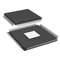
AD9910BSVZ Analog Devices Inc, AD9910BSVZ Datasheet - Page 52

AD9910BSVZ
Manufacturer Part Number
AD9910BSVZ
Description
IC DDS 1GSPS 14BIT PAR 100TQFP
Manufacturer
Analog Devices Inc
Datasheet
1.AD9910BSVZ-REEL.pdf
(64 pages)
Specifications of AD9910BSVZ
Design Resources
Synchronizing Multiple AD9910 1 GSPS Direct Digital Synthesizers (CN0121)
Resolution (bits)
14 b
Master Fclk
1GHz
Tuning Word Width (bits)
32 b
Voltage - Supply
1.8V, 3.3V
Operating Temperature
-40°C ~ 85°C
Mounting Type
Surface Mount
Package / Case
100-TQFP Exposed Pad, 100-eTQFP, 100-HTQFP, 100-VQFP
Pll Type
Frequency Synthesis
Frequency
1GHz
Supply Current
29mA
Supply Voltage Range
1.71V To 1.89V
Digital Ic Case Style
TQFP
No. Of Pins
100
Operating Temperature Range
-40°C To +85°C
Lead Free Status / RoHS Status
Lead free / RoHS Compliant
For Use With
AD9910/PCBZ - BOARD EVAL FOR AD9910 1GSPS
Lead Free Status / RoHS Status
Lead free / RoHS Compliant, Lead free / RoHS Compliant
Available stocks
Company
Part Number
Manufacturer
Quantity
Price
Company:
Part Number:
AD9910BSVZ
Manufacturer:
AVAGO
Quantity:
1 400
Company:
Part Number:
AD9910BSVZ
Manufacturer:
ADI
Quantity:
509
Company:
Part Number:
AD9910BSVZ
Manufacturer:
Analog Devices Inc
Quantity:
10 000
Part Number:
AD9910BSVZ
Manufacturer:
ADI/亚德诺
Quantity:
20 000
Company:
Part Number:
AD9910BSVZ-REEL
Manufacturer:
Analog Devices Inc
Quantity:
10 000
AD9910
Register
Name
(Serial
Address)
RAM
Profile 0
(0x0E)
Single Tone
Profile 1
(0x0F)
RAM
Profile 1
(0x0F)
Single Tone
Profile 2
(0x10)
RAM
Profile 2
(0x10)
Bit Range
(Internal
Address)
63:56
55:48
47:40
39:32
31:24
23:16
15:8
7:0
63:56
55:48
47:40
39:32
31:24
23:16
15:8
7:0
63:56
55:48
47:40
39:32
31:24
23:16
15:8
7:0
63:56
55:48
47:40
39:32
31:24
23:16
15:8
7:0
63:56
55:48
47:40
39:32
31:24
23:16
15:8
7:0
Bit 7
(MSB)
RAM Profile 0 waveform
RAM Profile 1 waveform
RAM Profile 1 waveform
RAM Profile 2 waveform
RAM Profile 2 waveform
RAM Profile 0 waveform
start address[1:0]
start address[1:0]
start address[1:0]
end address[1:0]
end address[1:0]
end address[1:0]
Open
Open
Open
Open
Open
Bit 6
Bit 5
No-dwell
high
No-dwell
high
No-dwell
high
RAM Profile 0 waveform start address[9:2]
RAM Profile 1 waveform start address[9:2]
RAM Profile 2 waveform start address[9:2]
RAM Profile 0 waveform end address[9:2]
RAM Profile 1 waveform end address[9:2]
RAM Profile 2 waveform end address[9:2]
RAM Profile 0 address step rate[15:8]
RAM Profile 1 address step rate[15:8]
RAM Profile 2 address step rate[15:8]
Rev. C | Page 52 of 64
RAM Profile 0 address step rate[7:0]
RAM Profile 1 address step rate[7:0]
RAM Profile 2 address step rate[7:0]
Frequency Tuning Word 1[31:24]
Frequency Tuning Word 1[23:16]
Frequency Tuning Word 2[31:24]
Frequency Tuning Word 2[23:16]
Frequency Tuning Word 1[15:8]
Frequency Tuning Word 2[15:8]
Frequency Tuning Word 1[7:0]
Frequency Tuning Word 2[7:0]
Amplitude Scale Factor 1[7:0]
Amplitude Scale Factor 2[7:0]
Phase Offset Word 1[15:8]
Phase Offset Word 2[15:8]
Bit 4
Open
Phase Offset Word 1[7:0]
Open
Phase Offset Word 2[7:0]
Open
Open
Open
Open
Amplitude Scale Factor 1[13:8]
Amplitude Scale Factor 2[13:8]
Bit 3
Zero-
crossing
Zero-
crossing
Zero-
crossing
Open
Open
Open
Open
Open
Open
Bit 2
RAM Profile 0 mode control[2:0]
RAM Profile 1 mode control[2:0]
RAM Profile 2 mode control[2:0]
Bit 1
Bit 0 (LSB)
Default
Value
(Hex)
0x00
0x00
0x00
0x00
0x00
0x00
0x00
0x00
0x00
0x00
0x00
0x00
0x00
0x00
0x00
0x00
0x00
0x00
0x00
0x00
0x00
0x00
0x00
0x00
0x00
0x00
0x00
0x00
0x00
0x00
0x00
0x00
0x00
0x00
0x00
0x00
0x00
0x00
0x00
0x00
1


