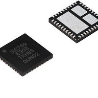
SIC779CD-T1-GE3 Vishay, SIC779CD-T1-GE3 Datasheet - Page 2

SIC779CD-T1-GE3
Manufacturer Part Number
SIC779CD-T1-GE3
Description
MOSFET & Power Driver ICs 40A 3-16V Built-In PWM Cont
Manufacturer
Vishay
Type
DrMOS Power Stager
Datasheet
1.SIC779CD-T1-GE3.pdf
(16 pages)
Specifications of SIC779CD-T1-GE3
Product
Half-Bridge Drivers
Rise Time
8 ns
Fall Time
8 ns
Propagation Delay Time
20 ns
Supply Voltage (max)
16 V
Supply Voltage (min)
3 V
Supply Current
400 uA
Maximum Power Dissipation
25 W
Maximum Operating Temperature
+ 125 C
Package / Case
MLP-66-40
Minimum Operating Temperature
- 40 C
Output Current
40 A
Output Voltage
5 V
Transistor Polarity
N-Channel
Lead Free Status / Rohs Status
Lead free / RoHS Compliant
SiC779
Vishay Siliconix
Note:
a. T
Stresses beyond those listed under "Absolute Maximum Ratings" may cause permanent damage to the device. These are stress ratings only,
and functional operation of the device at these or any other conditions beyond those indicated in the operational sections of the specifications is
not implied. Exposure to absolute maximum rating/conditions for extended periods may affect device reliability.
Note:
a. Recommended operating conditions are specified over the entire temperature range, and all voltages referenced to P
www.vishay.com
2
THE PRODUCTS DESCRIBED HEREIN AND THIS DOCUMENT ARE SUBJECT TO SPECIFIC DISCLAIMERS, SET FORTH AT
ORDERING INFORMATION
Part Number
SiC779CD-T1-GE3
SiC779DB
ABSOLUTE MAXIMUM RATINGS (T
Parameter
Input Voltage
Switch Node Voltage (DC)
Drive Input Voltage
Control Input Voltage
Logic Pins
Boot Voltage DC (referenced to C
Boot Voltage < 200 ns Transient (referenced to C
Boot to Phase Voltage DC
Boot to Phase Voltage < 200 ns
Ambient Temperature Range
Maximum Junction Temperature
Storage Junction Temperature
Soldering Peak Temperature
RECOMMENDED OPERATING CONDITIONS
Parameter
Input Voltage
Control Input Voltage
Drive Input Voltage
Switch Node
THERMAL RESISTANCE RATINGS
Parameter
Maximum Power Dissipation at T
Maximum Power Dissipation at T
Thermal Resistance from Junction to Top
Thermal Resistance from Junction to PCB
otherwise noted.
A
= 25 °C and all voltages referenced to P
PCB
PCB
GND
= 25 °C
= 100 °C
)
GND
This document is subject to change without notice.
= C
GND
Symbol
V
GND
A
V
)
SW_DC
V
V
DRV
CIN
= 25 °C, unless otherwise noted)
IN
unless otherwise noted.
V
V
PWM
THDN
Symbol
V
V
T
V
V
BS_PH
V
V
, V
Min.
T
DRV
T
STG
, V
SW
CIN
4.5
4.5
BS
IN
A
J
3
R
R
Symbol
P
DSBL#
P
SMOD
th_J_TOP
th_J_PCB
D_100C
D_25C
,
Typ.
Min.
- 0.3
- 0.3
- 0.3
- 0.3
- 0.3
- 0.3
- 0.3
- 0.3
- 0.3
- 40
- 65
12
12
PowerPAK MLP66-40
Typ.
Reference board
Package
V
CIN
Max.
Max.
5.5
5.5
125
150
150
260
16
16
S11-0703-Rev. B, 18-Apr-11
20
20
27
29
Max.
7
7
7
9
+ 0.3
25
10
15
5
Document Number: 67538
www.vishay.com/doc?91000
GND
= C
Unit
GND
Unit
°C/W
Unit
°C
V
V
W
unless


