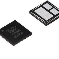
SIC779CD-T1-GE3 Vishay, SIC779CD-T1-GE3 Datasheet - Page 3

SIC779CD-T1-GE3
Manufacturer Part Number
SIC779CD-T1-GE3
Description
MOSFET & Power Driver ICs 40A 3-16V Built-In PWM Cont
Manufacturer
Vishay
Type
DrMOS Power Stager
Datasheet
1.SIC779CD-T1-GE3.pdf
(16 pages)
Specifications of SIC779CD-T1-GE3
Product
Half-Bridge Drivers
Rise Time
8 ns
Fall Time
8 ns
Propagation Delay Time
20 ns
Supply Voltage (max)
16 V
Supply Voltage (min)
3 V
Supply Current
400 uA
Maximum Power Dissipation
25 W
Maximum Operating Temperature
+ 125 C
Package / Case
MLP-66-40
Minimum Operating Temperature
- 40 C
Output Current
40 A
Output Voltage
5 V
Transistor Polarity
N-Channel
Lead Free Status / Rohs Status
Lead free / RoHS Compliant
Notes:
a. Typical limits are established by characterization and are not production tested.
b. Guaranteed by design.
Note:
a. Min. and Max. are not 100 % production tested.
Document Number: 67538
S11-0703-Rev. B, 18-Apr-11
THE PRODUCTS DESCRIBED HEREIN AND THIS DOCUMENT ARE SUBJECT TO SPECIFIC DISCLAIMERS, SET FORTH AT
ELECTRICAL SPECIFICATIONS
Parameter
Power Supplies
V
Drive Input Current (Dynamic)
Bootstrap Supply
Bootstrap Switch Forward Voltage
Control Inputs (PWM, DSBL#, SMOD)
PWM Rising Threshold
PWM Falling Threshold
PWM Tristate Rising Threshold
PWM Tristate Falling Threshold
PWM Tristate Rising Threshold Hysteresis
PWM Tristate Falling Threshold Hysteresis
Tristate Hold-Off Time
PWM Input Current
SMOD, DSBL# Logic Input Voltage
Pull Down Impedance
THDN Output Low
Protection
Thermal Warning Flag Set
Thermal Warning Flag Clear
Thermal Warning Flag Hysteresis
Under Voltage Lockout
Under Voltage Lockout
Under Voltage Lockout Hysteresis
High Side Gate Discharge Resistor
TIMING SPECIFICATIONS
Parameter
Turn Off Propagation Delay
High Side
Rise Time High Side
Fall Time High Side
Turn Off Propagation Delay
Low Side
Rise Time Low Side
Fall Time Low Side
Dead Time Rising
Dead Time Falling
CIN
Control Input Current
a
a
b
b
V
R
V
V
V
V
V
UVLO_HYST
V
V
HS_DSCRG
Symbol
Symbol
t
This document is subject to change without notice.
t
t
t
LOGIC_LH
LOGIC_LH
V
V
V
d_on_HS
R
d_off_LS
BS Diode
th_pwm_r
th_pwm_f
V
dead_on
dead_off
I
t
hys_tri_r
hys_tri_f
I
I
t
TSHO
THDNL
t
t
t
VDRV
th_tri_r
th_tri_f
VCIN
PWM
THDN
UVLO
r_HS
f_HS
r_LS
f_LS
V
Test Conditions Unless Specified
Test Conditions Unless Specified
V
VCIN
V
DSBL#
V
V
VDRV
25 % of PWM to 90 % of GH
75 % of PWM to 90 % of GL
IN
5 k resistor pull-up to V
VDRV
V
V
10 % of GL to 10 % of GH
10 % of GH to 10 % of GL
= 5 V, forward bias current 2 mA
DSBL#
DSBL#
V
V
= 12 V, V
f
f
s
VIN
DSBL#
Falling, off threshold
10 % to 90 % of GH
90 % to 10 % of GH
= 5 V, f
Rising, on threshold
10 % to 90 % of GL
90 % to 10 % of GL
s
Rising (low to high)
Falling (high to low)
= V
= 1000 kHz, D = 0.1
= V
= 300 kHz, D = 0.1
= 12 V, T
V
V
VCIN
T
= 0 V, no switching
= 5 V, no switching
VCIN
PWM
PWM
A
= V
s
VDRV
= 25 °C
= 300 kHz, D = 0.1
= 0 V; V
SMOD
= V
= 5 V
= 0 V
A
= V
DSBL#
= 25 °C
= 5 V,
VCIN
IN
= 12 V
= 5 V,
CIN
5 V,
Min.
Min.
3.5
0.8
0.9
3.4
2.5
10
10
2
Vishay Siliconix
www.vishay.com/doc?91000
Typ.
- 250
0.60
0.07
20.2
Typ.
400
600
300
170
150
250
150
135
400
3.8
1.0
1.3
3.7
3.3
2.9
60
15
48
40
15
20
20
15
15
15
8
8
8
a
www.vishay.com
Max.
Max.
SiC779
0.75
4.2
1.2
1.8
4.0
0.8
3.9
22
70
30
30
Unit
Unit
mV
mV
µA
mA
µA
k
ns
°C
ns
V
V
V
V
V
3


