SIC779CD-T1-GE3 Vishay, SIC779CD-T1-GE3 Datasheet - Page 7
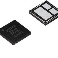
SIC779CD-T1-GE3
Manufacturer Part Number
SIC779CD-T1-GE3
Description
MOSFET & Power Driver ICs 40A 3-16V Built-In PWM Cont
Manufacturer
Vishay
Type
DrMOS Power Stager
Datasheet
1.SIC779CD-T1-GE3.pdf
(16 pages)
Specifications of SIC779CD-T1-GE3
Product
Half-Bridge Drivers
Rise Time
8 ns
Fall Time
8 ns
Propagation Delay Time
20 ns
Supply Voltage (max)
16 V
Supply Voltage (min)
3 V
Supply Current
400 uA
Maximum Power Dissipation
25 W
Maximum Operating Temperature
+ 125 C
Package / Case
MLP-66-40
Minimum Operating Temperature
- 40 C
Output Current
40 A
Output Voltage
5 V
Transistor Polarity
N-Channel
Lead Free Status / Rohs Status
Lead free / RoHS Compliant


PIN CONFIGURATION
Document Number: 67538
S11-0703-Rev. B, 18-Apr-11
THE PRODUCTS DESCRIBED HEREIN AND THIS DOCUMENT ARE SUBJECT TO SPECIFIC DISCLAIMERS, SET FORTH AT
PIN DESCRIPTION
8 to 14, PAD2
Pin Number
15, 29 to 35,
5, 37, PAD1
16 to 28
PAD3
36
38
39
40
1
2
3
4
6
7
Symbol
PHASE
DSBL#
SMOD
BOOT
THDN
V
C
P
PWM
V
V
GH
V
GL
SWH
GND
DRV
GND
CIN
IN
Disable low side gate operation. Active low.
This will be the bias supply input for control IC (5 V).
IC bias supply and gate drive supply voltage (5 V).
High side driver bootstrap voltage pin for external bootstrap capacitor.
Control signal ground. It should be connected to P
Gate signal output pin for high side MOSFET. Pin for monitoring.
Return pin for the HS bootstrap capacitor. Connect a 0.1 µF ceramic capacitor from this pin to the boot pin (4).
Input voltage for power stage. It is the drain of the high-side MOSFET.
It is the phase node between high side MOSFET source and low side MOSFET drain. It should be connected
to an output inductor. All pins internally connected.
Power ground.
Gate signal output pin for low side MOSFET. Pin for monitoring.
Thermal shutdown open drain output. Use a 10K pull up resistor to V
Disable pin. Active low.
PWM input logic signal. Compatible with Tristate controller function.
PHASE 7
SMOD 1
BOOT 4
C
V
Figure 5 - PowerPAK MLP 6 x 6 40P Pin Out - Top View
V
V
GND
DRV
GH 6
V
V
CIN
IN
This document is subject to change without notice.
IN
IN
10
2
3
5
8
9
A
V
P1
P2
GND
IN
V
SWH
P3
Description
GND
externally. All pins internally connected.
30 V
29 V
28 P
27 P
26 P
25 P
24 P
23 P
22 P
21 P
SWH
SWH
GND
GND
GND
GND
GND
GND
GND
GND
CIN
.
Vishay Siliconix
www.vishay.com/doc?91000
www.vishay.com
SiC779
7
Related parts for SIC779CD-T1-GE3
Image
Part Number
Description
Manufacturer
Datasheet
Request
R

Part Number:
Description:
Integrated Drmos Power Stage
Manufacturer:
Vishay
Datasheet:
Part Number:
Description:
357-036-542-201 CARDEDGE 36POS DL .156 BLK LOPRO
Manufacturer:
Vishay
Datasheet:
Part Number:
Description:
357-036-542-201 CARDEDGE 36POS DL .156 BLK LOPRO
Manufacturer:
Vishay
Datasheet:
Part Number:
Description:
357-036-542-201 CARDEDGE 36POS DL .156 BLK LOPRO
Manufacturer:
Vishay
Datasheet:
Part Number:
Description:
357-036-542-201 CARDEDGE 36POS DL .156 BLK LOPRO
Manufacturer:
Vishay
Datasheet:
Part Number:
Description:
357-036-542-201 CARDEDGE 36POS DL .156 BLK LOPRO
Manufacturer:
Vishay
Datasheet:
Part Number:
Description:
357-036-542-201 CARDEDGE 36POS DL .156 BLK LOPRO
Manufacturer:
Vishay
Datasheet:
Part Number:
Description:
357-036-542-201 CARDEDGE 36POS DL .156 BLK LOPRO
Manufacturer:
Vishay
Datasheet:
Part Number:
Description:
357-036-542-201 CARDEDGE 36POS DL .156 BLK LOPRO
Manufacturer:
Vishay
Datasheet:
Part Number:
Description:
357-036-542-201 CARDEDGE 36POS DL .156 BLK LOPRO
Manufacturer:
Vishay
Datasheet:
Part Number:
Description:
357-036-542-201 CARDEDGE 36POS DL .156 BLK LOPRO
Manufacturer:
Vishay
Datasheet:
Part Number:
Description:
357-036-542-201 CARDEDGE 36POS DL .156 BLK LOPRO
Manufacturer:
Vishay
Datasheet:
Part Number:
Description:
357-036-542-201 CARDEDGE 36POS DL .156 BLK LOPRO
Manufacturer:
Vishay
Datasheet:
Part Number:
Description:
357-036-542-201 CARDEDGE 36POS DL .156 BLK LOPRO
Manufacturer:
Vishay
Datasheet:
Part Number:
Description:
357-036-542-201 CARDEDGE 36POS DL .156 BLK LOPRO
Manufacturer:
Vishay
Datasheet: