DS26521LN+ Maxim Integrated Products, DS26521LN+ Datasheet - Page 103
DS26521LN+
Manufacturer Part Number
DS26521LN+
Description
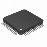
IC TXRX T1/E1/J1 64-LQFP
Manufacturer
Maxim Integrated Products
Type
Line Interface Units (LIUs)r
Datasheet
1.DS26521LN.pdf
(258 pages)
Specifications of DS26521LN+
Number Of Drivers/receivers
1/1
Protocol
T1/E1/J1
Voltage - Supply
3.135 V ~ 3.465 V
Mounting Type
Surface Mount
Package / Case
64-LQFP
Lead Free Status / RoHS Status
Lead free / RoHS Compliant


Register Name:
Description:
Register Address:
Bit #
Name
Default
Bits 5 and 4: Backplane Clock Select 1 and 0 (BPCLK[1:0]). These bits determine the clock frequency output on
the BPCLK pin.
Bit 3: Receive Loss of Signal/Signaling Freeze Select (RLOSSFS). This bit controls the function of the
AL/RSIGF/FLOS pin. The receive LOS is further selected between framer LOS and LIU LOS by GTCR2.2.
Bit 2: Receive Frame/Multiframe Sync Select (RFMSS). This bit controls the function of the RMSYNC/RFSYNC
pin.
Bit 1: Transmit Channel Block/Clock Select (TCBCS). This bit controls the function of the TCHBLK/CLK pin.
Bit 0: Receive Channel Block/Clock Select (RCBCS). This bit controls the function of the RCHBLK/CLK pin.
Register Name:
Register Description:
Register Address:
Bit #
Name
Default
Bit 2: LOS Selection (LOSS). If this bit is set, the AL/RSIGF/FLOS pin can be driven with LIU loss. If reset, the
pins can be driven by framer LOS. The selection of whether to drive AL/RSIGF/FLOS pin with LOS (analog or
digital) or signalling freeze is controlled by GFCR.2.
Bit 1: Transmit System Synchronization I/O Select (TSSYNCIOSEL). If this bit is set to a 1, the TSSYNCIO is
an 8kHz output synchronous to the BPCLK. This “frame pulse” can be used in conjunction with the backplane clock
to provide IBO signals for a system backplane. If this bit is reset, TSSYNCIO is an input. An 8kHz frame pulse is
required for transmit synchronization and IBO operation.
BPCLK1
0
0
1
1
0 = AL/RSIGF/FLOS pin outputs RLOS (receive loss)
1 = AL/RSIGF/FLOS pin outputs RSIGF (receive-signaling freeze)
0 = RMSYNC/RFSYNC pin outputs RFSYNC (receive frame sync)
1 = RMSYNC/RFSYNC pin outputs RMSYNC (receive multiframe sync)
0 = TCHBLK/CLK pin outputs TCHBLK (transmit channel block)
1 = TCHBLK/CLK pin outputs TCHCLK (transmit channel clock)
0 = RCHBLK/CLK pin outputs RCHBLK (receive channel block)
1 = RCHBLK/CLK pin outputs RCHCLK (receive channel clock)
—
7
0
BPCLK0
—
7
0
0
1
0
1
GFCR
Global Framer Control Register
0F1h
GTCR2
Global Transceiver Control Register 2
0F2h
—
6
0
—
6
0
BPCLK FREQUENCY
BPCLK1
16.384MHz
5
0
—
2.048MHz
4.096MHz
8.192MHz
5
0
BPCLK0
103 of 258
—
0
4
4
0
RFLOSSFS
—
3
0
3
0
LOSS
DS26521 Single T1/E1/J1 Transceiver
2
0
RFMSS
2
0
TSSYNCIOSEL
TCBCS
1
0
1
0
RCBCS
0
0
—
0
0
Related parts for DS26521LN+
Image
Part Number
Description
Manufacturer
Datasheet
Request
R

Part Number:
Description:
Ds26521 Single T1/e1/j1 Transceiver
Manufacturer:
Maxim Integrated Products, Inc.
Datasheet:
Part Number:
Description:
power light source LUXEON® Collimator
Manufacturer:
LUMILEDS [Lumileds Lighting Company]
Datasheet:

Part Number:
Description:
MAX7528KCWPMaxim Integrated Products [CMOS Dual 8-Bit Buffered Multiplying DACs]
Manufacturer:
Maxim Integrated Products
Datasheet:
Part Number:
Description:
Single +5V, fully integrated, 1.25Gbps laser diode driver.
Manufacturer:
Maxim Integrated Products
Datasheet:
Part Number:
Description:
Single +5V, fully integrated, 155Mbps laser diode driver.
Manufacturer:
Maxim Integrated Products
Datasheet:
Part Number:
Description:
VRD11/VRD10, K8 Rev F 2/3/4-Phase PWM Controllers with Integrated Dual MOSFET Drivers
Manufacturer:
Maxim Integrated Products
Datasheet:
Part Number:
Description:
Highly Integrated Level 2 SMBus Battery Chargers
Manufacturer:
Maxim Integrated Products
Datasheet:
Part Number:
Description:
Current Monitor and Accumulator with Integrated Sense Resistor; ; Temperature Range: -40°C to +85°C
Manufacturer:
Maxim Integrated Products
Part Number:
Description:
TSSOP 14/A°/RS-485 Transceivers with Integrated 100O/120O Termination Resis
Manufacturer:
Maxim Integrated Products
Part Number:
Description:
TSSOP 14/A°/RS-485 Transceivers with Integrated 100O/120O Termination Resis
Manufacturer:
Maxim Integrated Products
Part Number:
Description:
QFN 16/A°/AC-DC and DC-DC Peak-Current-Mode Converters with Integrated Step
Manufacturer:
Maxim Integrated Products
Part Number:
Description:
TDFN/A/65V, 1A, 600KHZ, SYNCHRONOUS STEP-DOWN REGULATOR WITH INTEGRATED SWI
Manufacturer:
Maxim Integrated Products
Part Number:
Description:
Integrated Temperature Controller f
Manufacturer:
Maxim Integrated Products
Part Number:
Description:
SOT23-6/I°/45MHz to 650MHz, Integrated IF VCOs with Differential Output
Manufacturer:
Maxim Integrated Products