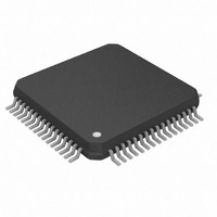
DS26521LN+ Maxim Integrated Products, DS26521LN+ Datasheet - Page 185

DS26521LN+
Manufacturer Part Number
DS26521LN+
Description
IC TXRX T1/E1/J1 64-LQFP
Manufacturer
Maxim Integrated Products
Type
Line Interface Units (LIUs)r
Datasheet
1.DS26521LN.pdf
(258 pages)
Specifications of DS26521LN+
Number Of Drivers/receivers
1/1
Protocol
T1/E1/J1
Voltage - Supply
3.135 V ~ 3.465 V
Mounting Type
Surface Mount
Package / Case
64-LQFP
Lead Free Status / RoHS Status
Lead free / RoHS Compliant
- Current page: 185 of 258
- Download datasheet (2Mb)
Register Name:
Register Description:
Register Address:
Bit #
Name
Default
Bit 7: Output Data Format (ODF).
Bit 6: Output Data Mode (ODM).
Bits 5 and 4: Transmit Clock Source Select 1 and 0 (TCSS[1:0]).
Bit 3: Multiframe Reference Select (MFRS). This bit selects the source for the transmit formatter multiframe
boundary.
Bit 2: Transmit Frame Mode Select (TFM) (T1 Mode Only).
Bit 1: Insert BPV (IBPV). A 0-to-1 transition on this bit will cause a single bipolar violation (BPV) to be inserted into
the transmit data stream. Once this bit has been toggled from 0 to 1, the device waits for the next occurrence of
three consecutive ones to insert the BPV. This bit must be cleared and set again for a subsequent error to be
inserted.
Bit 0 (T1 Mode): Transmit Loop Code Enable (TLOOP). See Section
Bit 0 (E1 Mode): CRC-4 Recalculate (CRC4R).
TCSS1
0
0
1
1
0 = bipolar data at TTIP and TRING
1 = NRZ data at TTIP; TRING = 0
0 = pulses at TTIP and TRING are one full TCLK period wide
1 = pulses at TTIP and TRING are one-half TCLK period wide
0 = Normal operation. Transmit multiframe boundary is determined by line-side counters referenced to
TSYNC when TSYNC is an input. Free-running when TSYNC is an output.
1 = Pass-forward operation. Transmit multiframe boundary determined by system-side counters referenced
to TSSYNCIO (input mode 3), which is then passed forward to the line-side clock domain. This mode can
only be used when the transmit elastic store is enabled with a synchronous backplane (i.e., no frame slips
allowed). This mode must be used to allow transmit hardware-signaling insertion while the transmit elastic
store is enabled.
0 = ESF framing mode
1 = D4 framing mode
0 = transmit data normally
1 = replace normal transmitted data with repeating code as defined in registers
0 = transmit CRC-4 generation and insertion operates in normal mode
1 = transmit CRC-4 generation operates according to G.706 Intermediate Path Recalculation method
TCSS0
ODF
ODF
0
1
0
1
7
0
The TCLK pin is always the source of transmit clock.
Switch to the clock present at RCLK when the signal at the TCLK pin fails to transition after
one channel time.
Reserved
Use the signal present at RCLK as the transmit clock. The TCLK pin is ignored.
TCR3
Transmit Control Register 3
183h
ODM
ODM
6
0
TCSS1
TCSS1
5
0
TCSS0
TCSS0
185 of 258
TRANSMIT CLOCK SOURCE
4
0
MFRS
MFRS
3
0
8.9.15
DS26521 Single T1/E1/J1 Transceiver
for details.
TFM
—
2
0
T1TCD1
IBPV
IBPV
1
0
and
T1TCD2
CRC4R
TLOOP
0
0
Related parts for DS26521LN+
Image
Part Number
Description
Manufacturer
Datasheet
Request
R

Part Number:
Description:
Ds26521 Single T1/e1/j1 Transceiver
Manufacturer:
Maxim Integrated Products, Inc.
Datasheet:

Part Number:
Description:
power light source LUXEON® Collimator
Manufacturer:
LUMILEDS [Lumileds Lighting Company]
Datasheet:

Part Number:
Description:
MAX7528KCWPMaxim Integrated Products [CMOS Dual 8-Bit Buffered Multiplying DACs]
Manufacturer:
Maxim Integrated Products
Datasheet:

Part Number:
Description:
Single +5V, fully integrated, 1.25Gbps laser diode driver.
Manufacturer:
Maxim Integrated Products
Datasheet:

Part Number:
Description:
Single +5V, fully integrated, 155Mbps laser diode driver.
Manufacturer:
Maxim Integrated Products
Datasheet:

Part Number:
Description:
VRD11/VRD10, K8 Rev F 2/3/4-Phase PWM Controllers with Integrated Dual MOSFET Drivers
Manufacturer:
Maxim Integrated Products
Datasheet:

Part Number:
Description:
Highly Integrated Level 2 SMBus Battery Chargers
Manufacturer:
Maxim Integrated Products
Datasheet:

Part Number:
Description:
Current Monitor and Accumulator with Integrated Sense Resistor; ; Temperature Range: -40°C to +85°C
Manufacturer:
Maxim Integrated Products

Part Number:
Description:
TSSOP 14/A°/RS-485 Transceivers with Integrated 100O/120O Termination Resis
Manufacturer:
Maxim Integrated Products

Part Number:
Description:
TSSOP 14/A°/RS-485 Transceivers with Integrated 100O/120O Termination Resis
Manufacturer:
Maxim Integrated Products

Part Number:
Description:
QFN 16/A°/AC-DC and DC-DC Peak-Current-Mode Converters with Integrated Step
Manufacturer:
Maxim Integrated Products

Part Number:
Description:
TDFN/A/65V, 1A, 600KHZ, SYNCHRONOUS STEP-DOWN REGULATOR WITH INTEGRATED SWI
Manufacturer:
Maxim Integrated Products

Part Number:
Description:
Integrated Temperature Controller f
Manufacturer:
Maxim Integrated Products

Part Number:
Description:
SOT23-6/I°/45MHz to 650MHz, Integrated IF VCOs with Differential Output
Manufacturer:
Maxim Integrated Products


