DS26521LN+ Maxim Integrated Products, DS26521LN+ Datasheet - Page 164
DS26521LN+
Manufacturer Part Number
DS26521LN+
Description
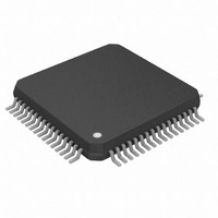
IC TXRX T1/E1/J1 64-LQFP
Manufacturer
Maxim Integrated Products
Type
Line Interface Units (LIUs)r
Datasheet
1.DS26521LN.pdf
(258 pages)
Specifications of DS26521LN+
Number Of Drivers/receivers
1/1
Protocol
T1/E1/J1
Voltage - Supply
3.135 V ~ 3.465 V
Mounting Type
Surface Mount
Package / Case
64-LQFP
Lead Free Status / RoHS Status
Lead free / RoHS Compliant


Register Name:
Register Description:
Register Address:
Bit #
Name
Default
Bit 7: Receive HDLC Data Bit 7 (RHD7). MSB of a HDLC packet data byte.
Bit 6: Receive HDLC Data Bit 6 (RHD6).
Bit 5: Receive HDLC Data Bit 5 (RHD5).
Bit 4: Receive HDLC Data Bit 4 (RHD4).
Bit 3: Receive HDLC Data Bit 3 (RHD3).
Bit 2: Receive HDLC Data Bit 2 (RHD2).
Bit 1: Receive HDLC Data Bit 1 (RHD1).
Bit 0: Receive HDLC Data Bit 0 (RHD0). LSB of a HDLC packet data byte.
Register Name:
Register Description:
Register Address:
Bit #
Name
Default
Bit 7 to 0: Receive Blank Channel Select for Channels 1 to 32 (CH[1:32]).
Note that when two or more sequential channels are chosen to be blanked, the receive-slip zone select bit should
be set to 0. If the blank channels are distributed (such as 1, 5, 9, 13, 17, 21, 25, 29), the RSZS bit can be set to 1,
which may provide a lower occurrence of slips in certain applications.
0 = Do not blank this channel (channel data is available on RSER)
1 = Data on RSER is forced to all ones for this channel
CH16
CH24
CH32
RHD7
CH8
7
0
7
0
CH15
CH23
CH31
CH7
RHF
Receive HDLC FIFO Register
0B6h
RBCS1, RBCS2, RBCS3, RBCS4
Receive Blank Channel Select Registers 1 to 4
0C0h, 0C1h, 0C2h, 0C3h
6
0
RHD6
6
0
CH14
CH22
CH30
CH6
5
0
RHD5
5
0
CH13
CH21
CH29
CH5
4
0
164 of 258
RHD4
4
0
CH12
CH20
CH28
CH4
3
0
RHD3
3
0
CH11
CH19
CH27
CH3
2
0
DS26521 Single T1/E1/J1 Transceiver
RHD2
CH10
CH18
CH26
CH2
2
0
0
1
CH17
CH25
RHD1
CH1
CH9
0
0
1
0
RBCS1
RBCS2
RBCS3
RBCS4
(E1 Mode
Only)
RHD0
0
0
Related parts for DS26521LN+
Image
Part Number
Description
Manufacturer
Datasheet
Request
R

Part Number:
Description:
Ds26521 Single T1/e1/j1 Transceiver
Manufacturer:
Maxim Integrated Products, Inc.
Datasheet:
Part Number:
Description:
power light source LUXEON® Collimator
Manufacturer:
LUMILEDS [Lumileds Lighting Company]
Datasheet:

Part Number:
Description:
MAX7528KCWPMaxim Integrated Products [CMOS Dual 8-Bit Buffered Multiplying DACs]
Manufacturer:
Maxim Integrated Products
Datasheet:
Part Number:
Description:
Single +5V, fully integrated, 1.25Gbps laser diode driver.
Manufacturer:
Maxim Integrated Products
Datasheet:
Part Number:
Description:
Single +5V, fully integrated, 155Mbps laser diode driver.
Manufacturer:
Maxim Integrated Products
Datasheet:
Part Number:
Description:
VRD11/VRD10, K8 Rev F 2/3/4-Phase PWM Controllers with Integrated Dual MOSFET Drivers
Manufacturer:
Maxim Integrated Products
Datasheet:
Part Number:
Description:
Highly Integrated Level 2 SMBus Battery Chargers
Manufacturer:
Maxim Integrated Products
Datasheet:
Part Number:
Description:
Current Monitor and Accumulator with Integrated Sense Resistor; ; Temperature Range: -40°C to +85°C
Manufacturer:
Maxim Integrated Products
Part Number:
Description:
TSSOP 14/A°/RS-485 Transceivers with Integrated 100O/120O Termination Resis
Manufacturer:
Maxim Integrated Products
Part Number:
Description:
TSSOP 14/A°/RS-485 Transceivers with Integrated 100O/120O Termination Resis
Manufacturer:
Maxim Integrated Products
Part Number:
Description:
QFN 16/A°/AC-DC and DC-DC Peak-Current-Mode Converters with Integrated Step
Manufacturer:
Maxim Integrated Products
Part Number:
Description:
TDFN/A/65V, 1A, 600KHZ, SYNCHRONOUS STEP-DOWN REGULATOR WITH INTEGRATED SWI
Manufacturer:
Maxim Integrated Products
Part Number:
Description:
Integrated Temperature Controller f
Manufacturer:
Maxim Integrated Products
Part Number:
Description:
SOT23-6/I°/45MHz to 650MHz, Integrated IF VCOs with Differential Output
Manufacturer:
Maxim Integrated Products