Si5369-EVB Silicon Laboratories Inc, Si5369-EVB Datasheet - Page 10
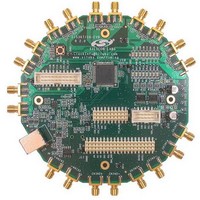
Si5369-EVB
Manufacturer Part Number
Si5369-EVB
Description
MCU, MPU & DSP Development Tools SI5369 DEV KIT
Manufacturer
Silicon Laboratories Inc
Specifications of Si5369-EVB
Processor To Be Evaluated
Si5369
Interface Type
I2C, SPI
Operating Supply Voltage
3.3 V
Lead Free Status / Rohs Status
Details


S i 5 3 6 5 / 6 6 - E V B
S i 5 3 6 7 / 6 8 - E V B
S i 5 3 6 9 - E V B
J14 is a three-pin by ten header that is used to establish input levels for the pin controlled two-level inputs using
jumper plugs. It also provides a means of externally driving the two-level input signals:
J8 is a 20 pin ribbon header that provides an external path to monitor the status pins.
J22 is a 10 pin ribbon header that provides an external path to serially communicate with the Any-Frequency
Precision Clock.
To control the Any-Frequency part that is on the Evaluation Board from an external serial port, open the Register
Programmer, connect to the Evaluation Board, go to Options in the top toolbar and select "Switch To External
Control Mode".
To control an Any-Frequency part that is on an external target board from the Evaluation Board using its serial port,
tie pin 9 of J22 low so that the on-board Any-Frequency part is constantly being held in reset. This will force it to
disable its SDA_SDO output buffer.
10
Table 4. Two-Level Input Jumper Header, J14
Table 5. External Status Connector, J8
J14.10B
J14.1B
J14.2B
J14.3B
J14.4B
J14.5B
J14.6B
J14.7B
J14.8B
J14.9B
J8.11
J8.13
J8.15
J8.17
J8.19
J8.1
J8.3
J8.5
J8.7
J8.9
J37
J36
FS_ALIGN
INT_ALRM
DUT_PWR
CK_CONF
CS0_C3A
CS1_C4A
CS0_C3A
CS1_C4A
DSBL34
FS_SW
Rev. 0.5
DEC
C1B
C2B
C3B
C1A
C2A
INC
LOL
Pin
Pin
—
—
Comment
Comment
not used
not used
CS0
CS1
C3A
C4A
Related parts for Si5369-EVB
Image
Part Number
Description
Manufacturer
Datasheet
Request
R

Part Number:
Description:
SMD/C°/SINGLE-ENDED OUTPUT SILICON OSCILLATOR
Manufacturer:
Silicon Laboratories Inc
Part Number:
Description:
Manufacturer:
Silicon Laboratories Inc
Datasheet:
Part Number:
Description:
N/A N/A/SI4010 AES KEYFOB DEMO WITH LCD RX
Manufacturer:
Silicon Laboratories Inc
Datasheet:
Part Number:
Description:
N/A N/A/SI4010 SIMPLIFIED KEY FOB DEMO WITH LED RX
Manufacturer:
Silicon Laboratories Inc
Datasheet:
Part Number:
Description:
N/A/-40 TO 85 OC/EZLINK MODULE; F930/4432 HIGH BAND (REV E/B1)
Manufacturer:
Silicon Laboratories Inc
Part Number:
Description:
EZLink Module; F930/4432 Low Band (rev e/B1)
Manufacturer:
Silicon Laboratories Inc
Part Number:
Description:
I°/4460 10 DBM RADIO TEST CARD 434 MHZ
Manufacturer:
Silicon Laboratories Inc
Part Number:
Description:
I°/4461 14 DBM RADIO TEST CARD 868 MHZ
Manufacturer:
Silicon Laboratories Inc
Part Number:
Description:
I°/4463 20 DBM RFSWITCH RADIO TEST CARD 460 MHZ
Manufacturer:
Silicon Laboratories Inc
Part Number:
Description:
I°/4463 20 DBM RADIO TEST CARD 868 MHZ
Manufacturer:
Silicon Laboratories Inc
Part Number:
Description:
I°/4463 27 DBM RADIO TEST CARD 868 MHZ
Manufacturer:
Silicon Laboratories Inc
Part Number:
Description:
I°/4463 SKYWORKS 30 DBM RADIO TEST CARD 915 MHZ
Manufacturer:
Silicon Laboratories Inc
Part Number:
Description:
N/A N/A/-40 TO 85 OC/4463 RFMD 30 DBM RADIO TEST CARD 915 MHZ
Manufacturer:
Silicon Laboratories Inc
Part Number:
Description:
I°/4463 20 DBM RADIO TEST CARD 169 MHZ
Manufacturer:
Silicon Laboratories Inc