Si5369-EVB Silicon Laboratories Inc, Si5369-EVB Datasheet - Page 4
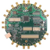
Si5369-EVB
Manufacturer Part Number
Si5369-EVB
Description
MCU, MPU & DSP Development Tools SI5369 DEV KIT
Manufacturer
Silicon Laboratories Inc
Specifications of Si5369-EVB
Processor To Be Evaluated
Si5369
Interface Type
I2C, SPI
Operating Supply Voltage
3.3 V
Lead Free Status / Rohs Status
Details


S i 5 3 6 5 / 6 6 - E V B
S i 5 3 6 7 / 6 8 - E V B
S i 5 3 6 9 - E V B
5. Functional Description
The Si5365/66-EVB, Si5367/68-EVB, Si5369-EVB, and DSPLLsim software allow for a complete and simple
evaluation of the functions, features, and performance of the Si536x Any-Frequency Precision Clocks.
5.1. Narrowband versus Wideband Operation
This document describes three evaluation boards: one for the Si5365 and Si5366, another for the Si5367 and
Si5368, and a third for the Si5369. The first evaluation board is for pin controlled clock parts, the second is for clock
parts that are to be controlled by an MCU over a serial port, and the third is for a very low loop bandwidth device
that is also controlled by an MCU. Two of the boards supports two parts: one that is wideband (the Si5365 and the
Si5367) and the one that is narrowband (the Si5366 and the Si5368). The third board only supports the low loop
bandwidth narrowband Si5369. The narrowband parts other than the Si5369 are both capable of operating in the
wideband mode, so evaluation of the wideband parts can be done by using a narrowband part in wideband mode.
As such, these evaluation boards are only populated with narrowband parts.
To evaluate Si5365 device operation using the Si5365/66-EVB, the RATE[1:0] pins must be set to HH using the
jumper provided. To evaluate Si5367 device operation using the Si5367/68-EVB, the Precision Clock EVB
Software should be configured for wideband mode. For details, see the Precision Clock EVB Software
documentation that can be found on the enclosed distribution CD.
5.2. Block Diagram
Figure 2 is a block diagram of the evaluation board. The MCU communicates to the host PC over a USB
connection. The MCU controls and monitors the Si536x through the CPLD. The CPLD, among other tasks,
translates the signals at the MCU voltage level of 3.3 V to the Si536x's voltage level, which is nominally 3.3, 2.5, or
1.8 V. The user has access to all of the Si536x's pins using the various jumper settings as well as through the host
PC via the MCU and CPLD.
4
DUT PWR
USB
+3.3 V
+1.8 V
Vreg
MCU
reg addr
ss
SPI bus
SPI bus
1.8 to 3.3 V
Figure 2. Si536x TQFP Block Diagram
Reset
switch
CPLD
LEDs
Input
SMAs
Rev. 0.5
Jumper
Headers
Terminate
Control signals
Ext RefClk
Si536x
CKOUT1
CKOUT2
CKOUT3
CKOUT4
FSOUT
SPI, I
status signals
2
C signals
Output
SMAs
Related parts for Si5369-EVB
Image
Part Number
Description
Manufacturer
Datasheet
Request
R

Part Number:
Description:
SMD/C°/SINGLE-ENDED OUTPUT SILICON OSCILLATOR
Manufacturer:
Silicon Laboratories Inc
Part Number:
Description:
Manufacturer:
Silicon Laboratories Inc
Datasheet:
Part Number:
Description:
N/A N/A/SI4010 AES KEYFOB DEMO WITH LCD RX
Manufacturer:
Silicon Laboratories Inc
Datasheet:
Part Number:
Description:
N/A N/A/SI4010 SIMPLIFIED KEY FOB DEMO WITH LED RX
Manufacturer:
Silicon Laboratories Inc
Datasheet:
Part Number:
Description:
N/A/-40 TO 85 OC/EZLINK MODULE; F930/4432 HIGH BAND (REV E/B1)
Manufacturer:
Silicon Laboratories Inc
Part Number:
Description:
EZLink Module; F930/4432 Low Band (rev e/B1)
Manufacturer:
Silicon Laboratories Inc
Part Number:
Description:
I°/4460 10 DBM RADIO TEST CARD 434 MHZ
Manufacturer:
Silicon Laboratories Inc
Part Number:
Description:
I°/4461 14 DBM RADIO TEST CARD 868 MHZ
Manufacturer:
Silicon Laboratories Inc
Part Number:
Description:
I°/4463 20 DBM RFSWITCH RADIO TEST CARD 460 MHZ
Manufacturer:
Silicon Laboratories Inc
Part Number:
Description:
I°/4463 20 DBM RADIO TEST CARD 868 MHZ
Manufacturer:
Silicon Laboratories Inc
Part Number:
Description:
I°/4463 27 DBM RADIO TEST CARD 868 MHZ
Manufacturer:
Silicon Laboratories Inc
Part Number:
Description:
I°/4463 SKYWORKS 30 DBM RADIO TEST CARD 915 MHZ
Manufacturer:
Silicon Laboratories Inc
Part Number:
Description:
N/A N/A/-40 TO 85 OC/4463 RFMD 30 DBM RADIO TEST CARD 915 MHZ
Manufacturer:
Silicon Laboratories Inc
Part Number:
Description:
I°/4463 20 DBM RADIO TEST CARD 169 MHZ
Manufacturer:
Silicon Laboratories Inc