Si5369-EVB Silicon Laboratories Inc, Si5369-EVB Datasheet
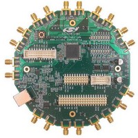
Si5369-EVB
Specifications of Si5369-EVB


Related parts for Si5369-EVB

Si5369-EVB Summary of contents
Page 1
... VCXO and loop filter components. The DSPLL loop bandwidth is digitally programmable, providing jitter performance optimization at the application level. Operating from a single 1.8, 2.5 ,or 3.3 V supply, the Si5369 is ideal for providing clock multiplication and jitter attenuation in high performance timing applications. Preliminary Rev. 0.4 5/11 This information applies to a product under development ...
Page 2
Functional Block Diagram CKIN1 ÷ N31 CKIN2 ÷ N32 CKIN3/FSYNC1 ÷ N33 CKIN4 ÷ N34 2 I C/SPI Port Rate Select Clock Select Skew Control Control FSYNC Realignment Device Interrupt LOL/LOS/FOS Alarms 2 Xtal or Refclock ÷ NC1_LS ® ÷ ...
Page 3
... Section 1. Electrical Specifications . . . . . . . . . . . . . . . . . . . . . . . . . . . . . . . . . . . . . . . . . . . . . . . . . . .4 2. Typical Phase Noise Performance . . . . . . . . . . . . . . . . . . . . . . . . . . . . . . . . . . . . . . . . . . 16 3. Functional Description . . . . . . . . . . . . . . . . . . . . . . . . . . . . . . . . . . . . . . . . . . . . . . . . . . . 20 3.1. External Reference . . . . . . . . . . . . . . . . . . . . . . . . . . . . . . . . . . . . . . . . . . . . . . . . . . 20 3.2. Further Documentation . . . . . . . . . . . . . . . . . . . . . . . . . . . . . . . . . . . . . . . . . . . . . . . 20 4. Pin Descriptions: Si5369 . . . . . . . . . . . . . . . . . . . . . . . . . . . . . . . . . . . . . . . . . . . . . . . . . .21 5. Register Map . . . . . . . . . . . . . . . . . . . . . . . . . . . . . . . . . . . . . . . . . . . . . . . . . . . . . . . . . . . . 26 6. Register Descriptions . . . . . . . . . . . . . . . . . . . . . . . . . . . . . . . . . . . . . . . . . . . . . . . . . . . .29 7. Ordering Guide . . . . . . . . . . . . . . . . . . . . . . . . . . . . . . . . . . . . . . . . . . . . . . . . . . . . . . . . . . 77 8. Package Outline: 100-Pin TQFP . . . . . . . . . . . . . . . . . . . . . . . . . . . . . . . . . . . . . . . . . . . . 78 9. Recommended PCB Layout . . . . . . . . . . . . . . . . . . . . . . . . . . . . . . . . . . . . . . . . . . . . . . . 79 10. Top Marking . . . . . . . . . . . . . . . . . . . . . . . . . . . . . . . . . . . . . . . . . . . . . . . . . . . . . . . . . . .81 Document Change List ...
Page 4
Electrical Specifications Table 1. Recommended Operating Conditions Parameter Symbol Ambient Temperature T A Supply Voltage during V DD Normal Operation Notes: 1. All minimum and maximum specifications are guaranteed and apply across the recommended operating conditions. Typical values apply ...
Page 5
Table 2. Absolute Limits Parameter DC Supply Voltage LVCMOS Input Voltage CKINn Voltage Level Limits XA/XB Voltage Level Limits Operating Junction Temperature Storage Temperature Range ESD HBM Tolerance (100 pF, 1.5 k); All pins except CKIN+/CKIN– ESD MM Tolerance; All ...
Page 6
Table 3. DC Characteristics (V = 1.8 ± 5%, 2.5 ±10%, or 3.3 V ±10 Parameter Symbol 1,6 Supply Current CKINn Input Pins Input Common Mode V ICM Voltage (Input Thresh- old Voltage) Input Resistance ...
Page 7
Table 3. DC Characteristics (Continued 1.8 ± 5%, 2.5 ±10%, or 3.3 V ±10 Parameter Symbol 3,5,6 Output Clocks (CKOUTn) Common Mode CKO VCM Differential Output CKO VD Swing Single Ended Output CKO VSE Swing Differential ...
Page 8
Table 3. DC Characteristics (Continued 1.8 ± 5%, 2.5 ±10%, or 3.3 V ±10 Parameter Symbol Output Drive Current CKO IO (CMOS driving into CKO for output low VOL or CKO for output VOH high. CKOUT+ ...
Page 9
Table 3. DC Characteristics (Continued 1.8 ± 5%, 2.5 ±10%, or 3.3 V ±10 Parameter Symbol 4 3-Level Input Pins Input Voltage Low V ILL Input Voltage Mid V IMM Input Voltage High V IHH Input ...
Page 10
Table 4. AC Specifications (V = 1.8 ± 5%, 2.5 ±10%, or 3.3 V ±10 Parameter Symbol Single-Ended Reference Clock Input Pin XA (XB with cap to GND) Input Resistance XA RIN Input Voltage Swing XA VPP Differential ...
Page 11
Table 4. AC Specifications (Continued 1.8 ± 5%, 2.5 ±10%, or 3.3 V ±10 Parameter Symbol Output Rise/Fall CKO TRF (20–80%) @ 212.5 MHz output Output Duty Cycle CKO DC Uncertainty @ 622.08 MHz LVCMOS Input ...
Page 12
Table 4. AC Specifications (Continued 1.8 ± 5%, 2.5 ±10%, or 3.3 V ±10 Parameter Symbol PLL Performance (fin = fout = 622.08 MHz 120 Hz; LVPECL) Lock Time t LOCKMP Settle Time t ...
Page 13
Table 5. Microprocessor Control (V = 1.8 ± 5%, 2.5 ±10%, or 3.3 V ±10 Parameter Symbol Bus Lines (SDA, SCL) Input Voltage Low VIL I2C Input Voltage High VIH I2C Input Current II I2C ...
Page 14
Table 5. Microprocessor Control (Continued 1.8 ± 5%, 2.5 ±10%, or 3.3 V ±10 Parameter Symbol SPI Specifications Duty Cycle, SCLK t DC Cycle Time, SCLK t c Rise Time, SCLK t r Fall Time, SCLK ...
Page 15
Table 6. Jitter Generation Parameter Symbol Measurement Jitter Gen JGEN 0.02–80 MHz OC-192 4–80 MHz 0.05–80 MHz Jitter Gen JGEN 0.12–20 MHz OC-48 *Note: Test conditions: 1. fIN = fOUT = 622.08 MHz 2. Clock input: LVPECL 3. Clock output: ...
Page 16
Typical Phase Noise Performance Jitter Bandwidth MHz Note: Number of samples: 8.91E9 16 Figure 3. Broadcast Video Jitter (peak-peak) 5.24 ps Preliminary Rev. 0.4 Jitter (RMS) 484 ...
Page 17
Note: Phase noise plot uses brick wall integration. Jitter Bandwidth SONET_OC48, 12 kHz to 20 MHz SONET_OC192_A, 20 kHz to 80 MHz SONET_OC192_B, 4 MHz to 80 MHz SONET_OC192_C, 50 kHz to 80 MHz Brick Wall_800 MHz ...
Page 18
Figure 5. Wireless Base Station Phase Noise Jitter Bandwidth MHz Note: Number of samples: 8.91E9 18 Jitter (peak-peak) Jitter (RMS) 7.28 ps Preliminary Rev. 0.4 581 ...
Page 19
... DEC DEC Rate RATE[1:0] Control Mode (H) CMODE Reset RST Assumes differential LVPECL termination (3 clock inputs. *Note: Figure 7. Si5369 Typical Application Circuit (SPI Control Mode) Preliminary Rev. 0.4 Option 1: Option 2: Crystal Ext. Refclk 0.1 µF 0.1 µF 0.1 µF CKOUT1+ 100 ...
Page 20
... The Si5369 is a jitter-attenuating precision clock multiplier for applications requiring sub 1 ps rms jitter performance. The Si5369 accepts four clock inputs ranging from 2 kHz to 710 MHz and generates five clock outputs ranging from 2 kHz to 945 MHz and select frequencies to 1.4 GHz. The device provides virtually any frequency translation combination across this operating range ...
Page 21
Register Map All register bits that are not defined in this map should always be written with the specified Reset Values. The writing to these bits of values other than the specified Reset Values may result in undefined device ...
Page 22
Register N2_HS [2: 128 129 130 DIGHOLD- VALID 131 ...
Page 23
Register D7 D6 132 134 135 PARTNUM_RO [3:0] 136 RST_REG ICAL 137 138 139 LOS4_EN LOS3_EN [0:0] [0:0] 140 141 142 143 144 FOS4_FLG FOS3_FLG FOS2_FLG PARTNUM_RO [11:4] LOS4_EN [1:1] LOS2_EN LOS1_EN FOS4_EN [0:0] [0:0] INDEPENDENTSKEW1 [7:0] ...
Page 24
Register Descriptions Register 0. Bit D7 D6 FREE_RUN CKOUT_ALWAYS_ON Name R R/W Type Reset value = 0001 0100 Bit Name 7 Reserved 6 FREE_RUN Free Run. Internal to the device, route XA/XB to CKIN2. This allows the device to ...
Page 25
Register 1. Bit D7 D6 CK_PRIOR4 [1:0] Name R/W Type Reset value = 1110 0100 Bit Name 7:6 CK_PRIOR4 [1:0] CK_PRIOR 4. Selects which of the input clocks will be 4th priority in the autoselection state machine. 00: CKIN0 is ...
Page 26
Register 2. Bit D7 D6 BWSEL_REG [3:0] Name R/W Type Reset value = 0100 0010 Bit Name 7:4 BWSEL_REG [3:0] BWSEL_REG. Selects nominal f3dB bandwidth for PLL. See the DSPLLsim for settings. After BWSEL_REG is written with a new value, ...
Page 27
Register 4. Bit D7 D6 AUTOSEL_REG [1:0] Name R/W Type Reset value = 0001 0010 Bit Name 7:6 AUTOSEL_REG [1:0] AUTOSEL_REG [1:0]. Selects method of input clock selection to be used. 00: Manual (either register or pin controlled. See CKSEL_PIN). ...
Page 28
Register 5. Bit D7 D6 ICMOS [1:0] Name R/W Type Reset value = 1110 1101 Bit Name 7:6 ICMOS [1:0] ICMOS [1:0]. When the output buffer is set to CMOS mode, these bits determine the output buf- fer drive strength. ...
Page 29
Register 6. Bit D7 D6 Name R R Type Reset value = 0010 1100 Bit Name 7:6 Reserved 5:3 SFOUT4_REG [2:0] SFOUT4_REG [2:0]. Controls output signal format and disable for CKOUT4 output buffer. The LVPECL and CMOS output formats draw ...
Page 30
Register 7. Bit D7 D6 Reserved Name R Type Reset value = 0010 1010 Bit Name 7:6 Reserved. 5:3 SFOUT5_REG [2:0] SFOUT5_REG [2:0] Controls output signal format and disable for CKOUT5 output buffer. The LVPECL and CMOS output formats draw ...
Page 31
Register 8. Bit D7 D6 HLOG_4[1:0] Name R/W Type Reset value = 0000 0000 Bit Name 7:6 HLOG_4 [1:0] HLOG_4 [1:0]. 00: Normal operation 01: Holds CKOUT4 output at static logic 0. Entrance and exit from this state will occur ...
Page 32
Register 9. Bit D7 D6 HIST_AVG [4:0] Name Type Reset value = 1100 0000 Bit Name 7:3 HIST_AVG [4:0] HIST_AVG [4:0]. Selects amount of averaging time to be used in generating MHIST, the value of M used during digital hold. ...
Page 33
Register 10. Bit DSBL5_REG Name R R/W R Type Reset value = 0000 0000 Bit Name 7:6 Reserved 5 DSBL5_REG DSBL5_REG. This bit controls the powerdown and disable of the CKOUT5 output buffer. If disable mode is ...
Page 34
Register 11. Bit D7 D6 Name R R Type Reset value = 0100 0000 Bit Name 7:4 Reserved 3 PD_CK4 PD_CK4. This bit controls the powerdown of the CKIN4 input buffer. 0: CKIN4 enabled 1: CKIN4 disabled 2 PD_CK3 PD_CK3. ...
Page 35
Register 19. Bit D7 D6 FOS_EN FOS_THR [1:0] Name R/W R/W Type Reset value = 0010 1100 Bit Name 7 FOS_EN FOS_EN. Frequency offset enable globally disables FOS. See the individual FOS enables (FOSx_EN, register 139). 00: FOS disable 01: ...
Page 36
Register 20. Bit ALRMOUT_PIN CK3_BAD_PIN CK2_BAD_PIN CK1_BAD_PIN LOL_PIN Name R R R/W Type Reset value = 0011 1100 Bit Name 7:6 Reserved 5 ALRMOUT_PIN ALRMOUT_PIN. The ALRMOUT status can be reflected on the ALRMOUT output pin. The ...
Page 37
Register 21. Bit CK4_ACTV_PIN CK3_ACTV_PIN CK2_ACTV_PIN CK1_ACTV_PIN Name R/W Type Reset value = 1111 1111 Bit Name 7:5 Reserved 4 CK4_ACTV_PIN CK4_ACTV_PIN. If the CKSEL[1]/CK4_ACTV pin is functioning as the CK4_ACTV output (see ...
Page 38
Register 22. Bit Name Type Reset value = 1101 1111 Bit Name 7:4 Reserved 3 CK_ACTV_ POL CK_ACTV_POL. Sets the active polarity for the CK1_ACTV, CK2_ACTV, CK3_ACTV, and CK4_ACTV signals when reflected on an ...
Page 39
Register 23. Bit LOS4_MSK Name Type Reset value = 0001 1111 Bit Name 7:5 Reserved 4 LOS4_MSK LOS4_MSK. Determines if a LOS on CKIN4 (LOS4_FLG) is used in the generation of an interrupt. Writes ...
Page 40
Register 24. Bit Name Type Reset value = 0011 1111 Bit Name 7:5 Reserved 4 FOS4_MSK FOS4_MSK. Determines if the FOS4_FLG is used to in the generation of an interrupt. Writes to this register ...
Page 41
Register 25. Bit D7 D6 N1_HS [2:0] Name R/W Type Reset value = 0010 0000 Bit Name 7:5 N1_HS [2:0] N1_HS [2:0]. Sets value for N1 high speed divider which drives NCn_LS ( low-speed divider. 000: ...
Page 42
Register 27. Bit D7 D6 Name Type Reset value = 0011 0001 Bit Name 7:0 NC1_LS [7:0] NC1_LS [7:0]. See Register 25. Register 28. Bit D7 D6 Name R R Type Reset value = 0000 0000 Bit Name 7:4 Reserved ...
Page 43
Register 29. Bit D7 D6 Name Type Reset value = 0000 0000 Bit Name 7:0 NC2_LS [15:8] NC2_LS [15:8]. See Register 28. Register 30. Bit D7 D6 Name Type Reset value = 0011 0001 Bit Name 7:0 NC2_LS [7:0] NC2_LS ...
Page 44
Register 31. Bit D7 D6 Name R R Type Reset value = 0000 0000 Bit Name 7:4 Reserved 3:0 NC3_LS [19:0] NC3_LS [19:0. Sets value for NC3 low-speed divider, which drives CKOUT3 output. Must odd. 00000000000000000000 = ...
Page 45
Register 33. Bit D7 D6 Name Type Reset value = 0011 0001 Bit Name 7:0 NC3_LS [7:0] NC3_LS [7:0]. See Register 31. Register 34. Bit D7 D6 Name R R Type Reset value = 0000 0000 Bit Name 7:4 Reserved ...
Page 46
Register 35. Bit D7 D6 Name Type Reset value = 0000 0000 Bit Name 7:0 NC4_LS [15:8] NC4_LS [15:8]. See Register 34. Register 36. Bit D7 D6 Name Type Reset value = 0011 0001 Bit Name 7:0 NC4_LS [7:0] NC4_LS ...
Page 47
Register 37. Bit D7 D6 Name R R Type Reset value = 0000 0000 Bit Name 7:4 Reserved 3:0 NC5_LS [19:0] NC5_LS [19:0]. Sets value for NC5 low-speed divider, which drives CKOUT5 output. Must odd. When CK_CONFIG=0: ...
Page 48
Register 39. Bit D7 D6 Name Type Reset value = 0011 0001 Bit Name 7:0 NC5_LS [7:0] NC5_LS [7:0]. See Register 37. Register 40. Bit D7 D6 N2_HS [2:0] Name R/W Type Reset value = 1100 0000 Bit Name 7:5 ...
Page 49
Register 41. Bit D7 D6 Name Type Reset value = 0000 0000 Bit Name 7:0 N2_LS [15:8] N2_LS [15:8]. See Register 40. Register 42. Bit D7 D6 Name Type Reset value = 1111 1001 Bit Name 7:0 N2_LS [7:0] N2_LS ...
Page 50
Register 44. Bit D7 D6 Name Type Reset value = 0000 0000 Bit Name 7:0 N31 [15:8] N31 [15:8]. See Register 43. Register 45. Bit D7 D6 Name Type Reset value = 0000 1001 Bit Name 7:0 N31 [7:0] N31 ...
Page 51
Register 46. Bit D7 D6 Name R R Type Reset value = 0000 0000 Bit Name 7:3 Reserved 2:0 N32_[18:0] N32_[18:0]. Sets value for input divider for CKIN2. 0000000000000000000 = 1 0000000000000000001 = 2 0000000000000000010 = 3 ... 1111111111111111111 = ...
Page 52
Register 48. Bit D7 D6 Name Type Reset value = 0000 1001 Bit Name 7:0 N32_[7:0] N32_[7:0]. See Register 46. Register 49. Bit D7 D6 Name R R Type Reset value = 0000 0000 Bit Name 18:0 N33_[18:0] N33_[18:0]. Sets ...
Page 53
Register 50. Bit D7 D6 Name Type Reset value = 0000 0000 Bit Name 7:0 N33_[15:8] N33_[15:8]. See Register 49. Register 51. Bit D7 D6 Name Type Reset value = 0000 1001 Bit Name 7:0 N33_[7:0] N33_[7:0]. See Register 49. ...
Page 54
Register 52. Bit D7 D6 Name R R Type Reset value = 0000 0000 Bit Name 7:3 Reserved 2:0 N34_[18:0] N34_[18:0]. Sets value for input divider for CKIN4. 0000000000000000000 = 1 0000000000000000001 = 2 0000000000000000010 = 3 ... 1111111111111111111 = ...
Page 55
Register 54. Bit D7 D6 Name Type Reset value = 0000 1001 Bit Name 7:0 N34_[15:8] N34_[7:0]. See Register 52. Register 55. Bit D7 D6 Name R R Type Reset value = 0000 0000 Bit Name 7:6 Reserved 5:3 CLKIN2RATE[2:0] ...
Page 56
Register 56. Bit D7 D6 Name R R Type Reset value = 0000 0000 Bit Name 7:6 Reserved 5:3 CLKIN4RATE[2:0] CLKIN4RATE[2:0]. CKINn frequency selection for FOS alarm monitoring. 000: 10–27 MHz 001: 25–54 MHz 002: 50–105 MHz 003: 95–215 MHz ...
Page 57
Register 128. Bit Name Type Reset value = 0010 0000 Bit Name 7:4 Reserved 3 CK4_ACTV_REG CK4_ACTV_REG. Indicates if CKIN4 is currently the active clock for the PLL input. 0: CKIN4 is ...
Page 58
Register 129. Bit D7 D6 Name R R Type Reset value = 0001 1110 Bit Name 7:5 Reserved 4 LOS4_INT LOS4_INT. Indicates the LOS status on CKIN4. 0: Normal operation. 1: Internal loss-of-signal alarm on CKIN4 input. 3 LOS3_INT LOS3_INT. ...
Page 59
Register 130. Bit D7 D6 DIGHOLDVALID Name R R Type Reset value = 0000 0001 Bit Name 7 Reserved 6 DIGHOLDVALID Digital Hold Valid. Indicates if the digital hold circuit has enough samples of a valid clock to meet digital ...
Page 60
Register 131. Bit Name Type Reset value = 0001 1111 Bit Name 7:5 Reserved 4 LOS4_FLG LOS4_FLG. CKIN4 Loss-of-Signal Flag. 0: Normal operation. 1: Held version of LOS4_INT. Generates active output interrupt if output ...
Page 61
Register 132. Bit D7 D6 FOS4_FLG FOS3_FLG FOS2_FLG FOS1_FLG Name R R Type Reset value = 0000 0010 Bit Name 7:6 Reserved 5 FOS4_FLG FOS4_FLG. CLKIN_4 Frequency Offset Flag. 0: Normal operation. 1: Held version of FOS4_INT. Generates active output ...
Page 62
... Register 134. Bit D7 D6 Name Type Reset value = 0000 0100 Bit Name 7:0 PARTNUM_RO [11:0] PARTNUM_RO [11:0]. Device ID: 0000 0100 0100'b=Si5369 Register 135. Bit D7 D6 PARTNUM_RO [3:0] Name R Type Reset value = 0100 0010 Bit Name 7:4 PARTNUM_RO [3:0] PARTNUM_RO [3:0]. See Register 134. ...
Page 63
Register 136. Bit D7 D6 RST_REG ICAL Name R/W R/W Type Reset value = 0000 0000 Bit Name 7 RST_REG RST_REG. Internal Reset. 0: Normal operation. 1: Reset of all internal logic. Outputs tristated or disabled during reset. 6 ICAL ...
Page 64
Register 137. Bit D7 D6 Name Type Reset value = 0000 0000 Bit Name 7:1 Reserved Do not modify. 0 FASTLOCK This bit must be set enable FASTLOCK. This improves initial lock time by dynamically changing the ...
Page 65
LOS2_EN [1:0] LOS2_EN [1:0]. Note: LOS1_EN is split between two registers. 00: Disable LOS monitoring. 01: Reserved. 10: Enable LOSA monitoring. 11: Enable LOS monitoring. LOSA is a slower and less sensitive version of LOS. See the Family Reference ...
Page 66
Register 139. Bit D7 D6 Name LOS4_EN [0:0] LOS3_EN [0:0] LOS2_EN [0:0] LOS1_EN [0:0] FOS4_EN FOS3_EN R/W R/W Type Reset value = 1111 1111 Bit Name 7 LOS4_EN [0:0] LOS4_EN [0:0]. Enable CKIN1 LOS Monitoring on the Specified Input (1 ...
Page 67
Bit Name 3 FOS4_EN FOS4_EN. Enables FOS on a Per Channel Basis. 0: Disable FOS monitoring. 1: Enable FOS monitoring. 2 FOS3_EN FOS3_EN. Enables FOS on a Per Channel Basis. 0: Disable FOS monitoring. 1: Enable FOS monitoring. 1 FOS2_EN ...
Page 68
Register 141. Bit D7 D6 Name Type Reset value = 0000 0001 Bit Name 7:0 INDEPENDENTSKEW2[7:0] INDEPENDENTSKEW2. Register 142. Bit D7 D6 Name Type Reset value = 0000 0000 Bit Name 7:0 INDEPENDENTSKEW3[7:0] INDEPENDENTSKEW3 . Register 143. Bit D7 D6 ...
Page 69
Register 144. Bit D7 D6 Name Type Reset value = 0000 0000 Bit Name 7:0 INDEPENDENTSKEW5[7:0] INDEPENDENTSKEW5 INDEPENDENTSKEW5[7:0] R/W Function 8 bit field that represents a twos complement of the phase offset in terms of clocks from ...
Page 70
Table 8. CKOUT_ALWAYS_ON and SQICAL Truth Table CKOUT_ALWAYS_ON SQICAL Table 9 lists all of the register locations that should be followed by an ICAL after their contents are changed. Table 9. Register ...
Page 71
Table 9. Register Locations Requiring ICAL Addr Register 40 N2_HS 40 N2_LS 43 N31 46 N32 49 N33 51 N34 55 CLKIN2RATE 55 CLKIN1RATE 56 CLKIN4RATE 56 CLKIN3RATE Preliminary Rev. 0.4 71 ...
Page 72
... GND 18 GND GND Pin # Pin Name I 20, NC 22, 23, 24, 25, 37, 47, 48, 50, 51, 52, 53, 56, 66, 67, 72, 73, 74, 75, 80, 85 RST Note: Internal register names are indicated by underlined italics, e.g., INT_PIN. See Si5369 Register Map Si5369 GND PAD Table 10. Si5369 Pin Descriptions Signal Level No Connect ...
Page 73
... O 10 C2B O 11 C3B O 12 INT_ALM O Note: Internal register names are indicated by underlined italics, e.g., INT_PIN. See Si5369 Register Map. Supply The device operates from a 1.8, 2.5, or 3.3 V supply. Bypass capacitors should be associated with the following V Pins Bypass Cap 5, 6 0.1 µF 15 0.1 µ ...
Page 74
... CKIN3– 44 CKIN1 CKIN1– Note: Internal register names are indicated by underlined italics, e.g., INT_PIN. See Si5369 Register Map. 74 Signal Level LVCMOS Input Clock Select/CKIN3 or CKIN4 Active Clock Indicator. Input: If manual clock selection is chosen, and if CKSEL_PIN = 1, the CKSEL pins control clock selection and the CKSEL_REG bits are ignored ...
Page 75
... A2_SS I 71 SDI I Note: Internal register names are indicated by underlined italics, e.g., INT_PIN. See Si5369 Register Map. LVCMOS PLL Loss of Lock Indicator. This pin functions as the active high PLL loss of lock indicator if the LOL_PIN register bit is set to one PLL locked PLL unlocked. ...
Page 76
... CKOUT4– CKOUT4+ GND PAD GND PAD GND Note: Internal register names are indicated by underlined italics, e.g., INT_PIN. See Si5369 Register Map. 76 Signal Level MULTI Clock Output 3. Differential clock output. Output signal format is selected by SFOUT3_REG register bits. Output is differential for LVPECL, LVDS, and CML compatible modes ...
Page 77
... MHz 1.213–1.417 GHz Si5369B-C-GQ 2 kHz–808 MHz Si5369C-C-GQ 2 kHz–346 MHz Si5369D-C-GQ 2 kHz–243 MHz Note: Add the end of the device to denote tape and reel options (for example, Si5369-C-GMR). Package ROHS6, Pb-Free 100-Pin TQFP 100-Pin TQFP 100-Pin TQFP 100-Pin TQFP Preliminary Rev ...
Page 78
... Package Outline: 100-Pin TQFP Figure 8 illustrates the package details for the Si5369. Table 11 lists the values for the dimensions shown in the illustration. Figure 8. 100-Pin Thin Quad Flat Package (TQFP) Table 11. Dimension Min Nom A — A1 0.05 A2 0.95 1.00 b 0.17 0.22 c 0.09 D 16.00 BSC. ...
Page 79
Recommended PCB Layout Figure 9. PCB Land Pattern Diagram Preliminary Rev. 0.4 79 ...
Page 80
Table 12. PCB Land Pattern Dimensions Dimension Notes: General 1. All dimensions shown are in millimeters (mm) unless otherwise noted. 2. Dimensioning and Tolerancing is per the ...
Page 81
Top Marking Mark Method: Logo Size: Font Size: Line 1 Marking: Line 2 Marking: Line 3 Marking: Laser 9.2 x 3.1 mm Center-Justified 3.0 Point (1.07 mm) Right-Justified Device Part Number See "7. Ordering Guide" on page ...
Page 82
OCUMENT HANGE IST Revision 0.1 to Revision 0.4 Updated Table 4, “AC Specifications,” on page 10. Added table note. 82 Preliminary Rev. 0.4 ...
Page 83
N : OTES Preliminary Rev. 0.4 83 ...
Page 84
... Should Buyer purchase or use Silicon Laboratories products for any such unintended or unauthorized ap- plication, Buyer shall indemnify and hold Silicon Laboratories harmless against all claims and damages. Silicon Laboratories, Silicon Labs, and DSPLL are trademarks of Silicon Laboratories Inc. Other products or brandnames mentioned herein are trademarks or registered trademarks of their respective holders. ...