Si5369-EVB Silicon Laboratories Inc, Si5369-EVB Datasheet - Page 5
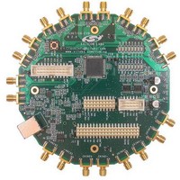
Si5369-EVB
Manufacturer Part Number
Si5369-EVB
Description
MCU, MPU & DSP Development Tools SI5369 DEV KIT
Manufacturer
Silicon Laboratories Inc
Specifications of Si5369-EVB
Processor To Be Evaluated
Si5369
Interface Type
I2C, SPI
Operating Supply Voltage
3.3 V
Lead Free Status / Rohs Status
Details


5.3. Si536x Input and Output Clocks
The Si536x has four differential inputs that are ac terminated to 50 and then ac coupled to the part. Single ended
operation can be implemented by simply not connecting to one of the two of the differential pairs. When operating
with clock inputs of 1 MHz or less in frequency, the appropriate dc blocking capacitors (C58, C61, C47, C50, C53,
C55, C42 and C45) located on the bottom of the board should be replaced with zero ohm resistors. The reason for
this is that the capacitive reactance of the ac coupling capacitors becomes significant at low frequencies. It is also
important that the CKIN signal meet the minumum rise time of 11 ns (CKNtrf) even though the input frequency is
low.
The four clock outputs are all differential, ac coupled and configured for driving 50 transmission lines. When
using single ended outputs, it is important that the unused half of the output be terminated. Given that the
Frame Sync signal can have a duty cycle that is far from 50%, the Frame Sync outputs are dc coupled. If the
Frame Sync or other clock ouputs signals are configured for CMOS, then the two outputs are not complements of
one another and should be wired in parallel so that the output drive current is doubled. To evaluate CMOS level
Frame Sync outputs, a 0 resistor should be installed at R19. Note that for the MCU controlled parts that support
Frame Sync mode (Si5367 and Si5368), the Frame Sync output signal format can be configured independently of
the other four outputs.
Two jumpers are provided to assist in monitoring the Si536x power. When R36 is removed, J25 can be used to
measure the device current. J18 can be used at any time to monitor the supply voltage at the device.
The Si5366, Si5368, and Si5369 require that an external reference clock be provided to enable the devices to
operate as narrowband jitter attenuators with loop bandwidths as low as 60 Hz (as low as 4 Hz for the Si5369). The
external reference clock can be either a crystal, a stand-alone oscillator or some other clock source. The range of
acceptable reference frequencies is described in the Any-Frequency Precision Clocks Family Reference Manual
(Si53xx-RM). The EVB's are shipped with a 3rd overtone 114.285 MHz crystal that is used in the majority of
applications. J1 and J2 are used when the Si536x is to be configured in narrowband mode with an external
reference oscillator (i.e., without using the 114.285 MHz crystal).
The RATE pins should also be configured for the desired mode, either through DSPLLsim or using the jumper
plugs at J17 (see Table 7 on page 11).
Table 2 shows how the various components should be configured for the three modes of operation:
For a differential external reference, connect the balanced input signals to J1 and J2. For single-ended operation,
connect the input signal to J1 and disconnect J2.
R51 is provided so that a different termination scheme can be used. If R51 is populated, then remove R52 and R24.
Notes:
Input 1
Input 2
1. Xtal is 114.285 MHz 3rd overtone.
2. For external reference frequencies and RATE pin settings, see the
3. NC—no connect.
4. NOPOP—do not install this component.
RATE0
RATE1
C39
C22
R50
R28
Any-Frequency Precision Clock Family Reference Manual
Table 2. Reference Input Mode
NOPOP
NOPOP
NOPOP
install
Xtal
NC
NC
M
M
3
1
4
Rev. 0.5
38.88 MHz Ext
NOPOP
NOPOP
Mode
install
install
Ref
J1
J2
—
—
2
Wideband
NOPOP
NOPOP
install
install
NC
NC
H
H
S i 5 3 6 5 / 6 6 - E V B
S i 5 3 6 7 / 6 8 - E V B
.
S i 5 3 6 9 - E V B
5
Related parts for Si5369-EVB
Image
Part Number
Description
Manufacturer
Datasheet
Request
R

Part Number:
Description:
SMD/C°/SINGLE-ENDED OUTPUT SILICON OSCILLATOR
Manufacturer:
Silicon Laboratories Inc
Part Number:
Description:
Manufacturer:
Silicon Laboratories Inc
Datasheet:
Part Number:
Description:
N/A N/A/SI4010 AES KEYFOB DEMO WITH LCD RX
Manufacturer:
Silicon Laboratories Inc
Datasheet:
Part Number:
Description:
N/A N/A/SI4010 SIMPLIFIED KEY FOB DEMO WITH LED RX
Manufacturer:
Silicon Laboratories Inc
Datasheet:
Part Number:
Description:
N/A/-40 TO 85 OC/EZLINK MODULE; F930/4432 HIGH BAND (REV E/B1)
Manufacturer:
Silicon Laboratories Inc
Part Number:
Description:
EZLink Module; F930/4432 Low Band (rev e/B1)
Manufacturer:
Silicon Laboratories Inc
Part Number:
Description:
I°/4460 10 DBM RADIO TEST CARD 434 MHZ
Manufacturer:
Silicon Laboratories Inc
Part Number:
Description:
I°/4461 14 DBM RADIO TEST CARD 868 MHZ
Manufacturer:
Silicon Laboratories Inc
Part Number:
Description:
I°/4463 20 DBM RFSWITCH RADIO TEST CARD 460 MHZ
Manufacturer:
Silicon Laboratories Inc
Part Number:
Description:
I°/4463 20 DBM RADIO TEST CARD 868 MHZ
Manufacturer:
Silicon Laboratories Inc
Part Number:
Description:
I°/4463 27 DBM RADIO TEST CARD 868 MHZ
Manufacturer:
Silicon Laboratories Inc
Part Number:
Description:
I°/4463 SKYWORKS 30 DBM RADIO TEST CARD 915 MHZ
Manufacturer:
Silicon Laboratories Inc
Part Number:
Description:
N/A N/A/-40 TO 85 OC/4463 RFMD 30 DBM RADIO TEST CARD 915 MHZ
Manufacturer:
Silicon Laboratories Inc
Part Number:
Description:
I°/4463 20 DBM RADIO TEST CARD 169 MHZ
Manufacturer:
Silicon Laboratories Inc