DS32512N# Maxim Integrated Products, DS32512N# Datasheet - Page 23
DS32512N#
Manufacturer Part Number
DS32512N#
Description
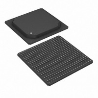
IC LIU DS3/E3/STS-1 484-BGA
Manufacturer
Maxim Integrated Products
Type
Line Interface Units (LIUs)r
Datasheet
1.DS32506N.pdf
(130 pages)
Specifications of DS32512N#
Protocol
DS3
Voltage - Supply
3.135 V ~ 3.465 V
Mounting Type
Surface Mount
Package / Case
484-BGA
Lead Free Status / RoHS Status
Lead free / RoHS Compliant
Number Of Drivers/receivers
-
Available stocks
Company
Part Number
Manufacturer
Quantity
Price


Table 7-9. JTAG Pin Descriptions
Table 7-10. Power-Supply Pin Descriptions
Table 7-11. Manufacturing Test Pin Descriptions
MT[10:0]
RVDDn
RVSSn
TVDDn
VDD18
VDD33
JVDDn
TVSSn
JTCLK
JVSSn
JTRST
NAME
NAME
CVDD
NAME
CVSS
JTMS
JTDO
JTDI
VSS
TYPE
TYPE
TYPE
Test
Ipu
Ipu
Ipu
Oz
P
P
P
P
P
P
P
P
P
P
P
I
Digital Core 1.8V Power, 1.8V ±5%
I/O 3.3V Power, 3.3V ±5%
Ground for VDD18 and VDD33
Jitter Attenuator 1.8V Power, 1.8V ±5%
Jitter Attenuator Ground
Receive 1.8V Power, 1.8V ±5%
Receive Ground
Transmit 1.8V Power, 1.8V ±5%
Transmit Ground
CLAD 1.8V ±5%
CLAD Ground
Manufacturing Test Pins 10 to 0. MT[0] and MT[2:10] must not be connected. MT[1]
must be connected to digital ground (same as VSS pins).
JTAG Clock. This pin shifts data into JTDI on the rising edge and out of JTDO on the
falling edge. JTCLK is typically a low frequency (less than 10MHz) 50% duty cycle clock
signal. If boundary scan is not used, JTCLK should be pulled high. See Section 10.
JTAG Mode Select. This pin is used to control the JTAG controller state machine. JTMS
is sampled on the rising edge of JTCLK. If boundary scan is not used, JTMS should be
left unconnected or pulled high. See Section 10.
JTAG Data Input. This pin is used to input data into the register that is enabled by the
JTAG controller state machine. JTDI is sampled on the rising edge of JTCLK. If boundary
scan is not used, JTDI should be left unconnected or pulled high. See Section 10.
JTAG Data Output. This pin is the output of an internal scan shift register enabled by
the JTAG controller state machine. JTDO is updated on the falling edge of JTCLK. JTDO
is in high-impedance mode when a register is not selected or when the
JTDO goes into and out of high-impedance mode after the falling edge of JTCLK. See
Section 10.
JTAG Reset (Active Low). When active, this pin forces the JTAG controller logic into
the reset state and forces the JTDO pin into high-impedance mode. The JTAG controller
is also reset when power is first applied via a power-on reset circuit.
high or low for normal operation, but must be high for JTAG operation. See Section 10.
23 of 130
FUNCTION
FUNCTION
FUNCTION
DS32506/DS32508/DS32512
JTRST
JTRST
can be driven
pin is low.
Related parts for DS32512N#
Image
Part Number
Description
Manufacturer
Datasheet
Request
R

Part Number:
Description:
IC LIU DS3/E3/STS-1 144-CSBGA
Manufacturer:
Maxim Integrated Products
Datasheet:

Part Number:
Description:
Network Controller & Processor ICs DS3-E3-STS-1 Line In terface Unit (LIU) S
Manufacturer:
Maxim Integrated Products
Part Number:
Description:
MAX7528KCWPMaxim Integrated Products [CMOS Dual 8-Bit Buffered Multiplying DACs]
Manufacturer:
Maxim Integrated Products
Datasheet:
Part Number:
Description:
Single +5V, fully integrated, 1.25Gbps laser diode driver.
Manufacturer:
Maxim Integrated Products
Datasheet:
Part Number:
Description:
Single +5V, fully integrated, 155Mbps laser diode driver.
Manufacturer:
Maxim Integrated Products
Datasheet:
Part Number:
Description:
VRD11/VRD10, K8 Rev F 2/3/4-Phase PWM Controllers with Integrated Dual MOSFET Drivers
Manufacturer:
Maxim Integrated Products
Datasheet:
Part Number:
Description:
Highly Integrated Level 2 SMBus Battery Chargers
Manufacturer:
Maxim Integrated Products
Datasheet:
Part Number:
Description:
Current Monitor and Accumulator with Integrated Sense Resistor; ; Temperature Range: -40°C to +85°C
Manufacturer:
Maxim Integrated Products
Part Number:
Description:
TSSOP 14/A°/RS-485 Transceivers with Integrated 100O/120O Termination Resis
Manufacturer:
Maxim Integrated Products
Part Number:
Description:
TSSOP 14/A°/RS-485 Transceivers with Integrated 100O/120O Termination Resis
Manufacturer:
Maxim Integrated Products
Part Number:
Description:
QFN 16/A°/AC-DC and DC-DC Peak-Current-Mode Converters with Integrated Step
Manufacturer:
Maxim Integrated Products
Part Number:
Description:
TDFN/A/65V, 1A, 600KHZ, SYNCHRONOUS STEP-DOWN REGULATOR WITH INTEGRATED SWI
Manufacturer:
Maxim Integrated Products
Part Number:
Description:
Integrated Temperature Controller f
Manufacturer:
Maxim Integrated Products
Part Number:
Description:
SOT23-6/I°/45MHz to 650MHz, Integrated IF VCOs with Differential Output
Manufacturer:
Maxim Integrated Products
Part Number:
Description:
SOT23-6/I°/45MHz to 650MHz, Integrated IF VCOs with Differential Output
Manufacturer:
Maxim Integrated Products