DS32512N# Maxim Integrated Products, DS32512N# Datasheet - Page 24
DS32512N#
Manufacturer Part Number
DS32512N#
Description
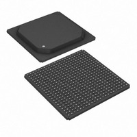
IC LIU DS3/E3/STS-1 484-BGA
Manufacturer
Maxim Integrated Products
Type
Line Interface Units (LIUs)r
Datasheet
1.DS32506N.pdf
(130 pages)
Specifications of DS32512N#
Protocol
DS3
Voltage - Supply
3.135 V ~ 3.465 V
Mounting Type
Surface Mount
Package / Case
484-BGA
Lead Free Status / RoHS Status
Lead free / RoHS Compliant
Number Of Drivers/receivers
-
Available stocks
Company
Part Number
Manufacturer
Quantity
Price


8. FUNCTIONAL DESCRIPTION
8.1 LIU Mode
Each port is independently configurable for DS3, E3 or STS-1 operation. When only the hardware interface is
enabled
enabled
8.2 Transmitter
8.2.1
If the jitter attenuator is not enabled in the transmit path, the signal on
transmission quality (i.e., ±20ppm frequency accuracy and low jitter). If the jitter attenuator is enabled in the
transmit path, the signal on
frequency within ±20ppm of the nominal line rate. When enabled in the transmit path, the jitter attenuator generates
the transmit line clock. See Section
The polarity of
Normally data is sampled on the
the falling edge of TCLK, pull the
8.2.1.1
When the
ignored. When the
comes from
one another, common transmit clocking reduces wiring complexity between the LIU and the neighboring framer or
mapper component.
8.2.2 Framer Interface Format and the B3ZS/HDB3 Encoder
Data to be transmitted can be input in either bipolar or binary format.
8.2.2.1
To select the bipolar interface format, pull the
bipolar format, the B3ZS/HDB3 encoder is disabled and the data to be transmitted is sampled on the
TNEG
TNEG
opposite state of the pulse previously transmitted.
8.2.2.2
To select the binary interface format, pull the
(per port). In binary format, the B3ZS/HBD3 encoder is enabled, and the NRZ data to be transmitted is sampled on
the
modes, B3ZS encoding is performed. In these modes, whenever three consecutive zeros are found in the transmit
data stream they are replaced with a B3ZS codeword. In E3 mode HDB3 encoding is performed. In this mode,
whenever four consecutive zeros are found in the transmit data stream they are replaced with an HDB3 codeword.
In all three modes, the B3ZS or HDB3 codeword is constructed such that the last bit is a BPV with the opposite
polarity of the most recently transmitted BPV.
8.2.3 Error Insertion
Bipolar violation (BPV) errors and excessive zeros (EXZ) errors can be inserted into the transmit data stream using
the transmit manual error insert (TMEI) logic (see Section 8.7.5). Configuration bit LINE.TCR:BPVI enables the
insertion of bipolar violations, while LINE.TCR:EXZI enables the insertion of excessive zero events. Note: BPV
errors and EXZ errors can only be inserted in the binary interface format.
If the transmitter is configured for binary interface format (Section 8.2.2.2) and BPVI = 1 then when the configured
manual error insert control goes from zero to one, the transmitter waits for the next occurrence of two consecutive
TDAT
pins. Positive-polarity pulses are indicated by
= 1. If
Transmit Clock
(IFSEL
(IFSEL
Transmit Common Clock Mode
Bipolar Interface Format
Binary Interface Format
TCC
pin. The
TCLKn
TPOS
≠ 000) the PORT.CR2:LM[1:0] control bits specify the LIU mode.
TCLK
pin is high, the transmit paths of all ports are clocked from TCLK1 and pins TCLKx (x ≠ 1) are
= 000 and
TCC
or TCLK1. In designs where the transmit paths of all ports can be clocked synchronously with
TNEG
and
can be inverted to support glueless interfacing to a variety of neighboring components.
pin is low, the PORT.CR2:TCC register bit specifies whether the transmit clock for port n
TNEG
pin is ignored in binary interface mode and should be wired low. In DS3 and STS-1
HW
TCLK
= 1), the
TPOS/TDAT
TCLKI
are high at the same time the transmitter generates an AMI pulse that is the
8.4
can be jittery and/or periodically gapped, but must still have an average
for more information about the jitter attenuator.
pin high or set the PORT.INV:TCLKI configuration bit.
LMn[1:0]
TBIN
and
TBIN
TNEG
pins specify the LIU mode. When a microprocessor interface is
pin high (all ports) or set the PORT.CR2:TBIN configuration bit
24 of 130
pin low and clear the PORT.CR2:TBIN configuration bit. In
TPOS
pins on the rising edge of TCLK. To sample these pins on
= 1, while negative-polarity pulses are indicated by
TCLK
is the transmit line clock and must be
DS32506/DS32508/DS32512
TPOS
and
Related parts for DS32512N#
Image
Part Number
Description
Manufacturer
Datasheet
Request
R

Part Number:
Description:
IC LIU DS3/E3/STS-1 144-CSBGA
Manufacturer:
Maxim Integrated Products
Datasheet:

Part Number:
Description:
Network Controller & Processor ICs DS3-E3-STS-1 Line In terface Unit (LIU) S
Manufacturer:
Maxim Integrated Products
Part Number:
Description:
MAX7528KCWPMaxim Integrated Products [CMOS Dual 8-Bit Buffered Multiplying DACs]
Manufacturer:
Maxim Integrated Products
Datasheet:
Part Number:
Description:
Single +5V, fully integrated, 1.25Gbps laser diode driver.
Manufacturer:
Maxim Integrated Products
Datasheet:
Part Number:
Description:
Single +5V, fully integrated, 155Mbps laser diode driver.
Manufacturer:
Maxim Integrated Products
Datasheet:
Part Number:
Description:
VRD11/VRD10, K8 Rev F 2/3/4-Phase PWM Controllers with Integrated Dual MOSFET Drivers
Manufacturer:
Maxim Integrated Products
Datasheet:
Part Number:
Description:
Highly Integrated Level 2 SMBus Battery Chargers
Manufacturer:
Maxim Integrated Products
Datasheet:
Part Number:
Description:
Current Monitor and Accumulator with Integrated Sense Resistor; ; Temperature Range: -40°C to +85°C
Manufacturer:
Maxim Integrated Products
Part Number:
Description:
TSSOP 14/A°/RS-485 Transceivers with Integrated 100O/120O Termination Resis
Manufacturer:
Maxim Integrated Products
Part Number:
Description:
TSSOP 14/A°/RS-485 Transceivers with Integrated 100O/120O Termination Resis
Manufacturer:
Maxim Integrated Products
Part Number:
Description:
QFN 16/A°/AC-DC and DC-DC Peak-Current-Mode Converters with Integrated Step
Manufacturer:
Maxim Integrated Products
Part Number:
Description:
TDFN/A/65V, 1A, 600KHZ, SYNCHRONOUS STEP-DOWN REGULATOR WITH INTEGRATED SWI
Manufacturer:
Maxim Integrated Products
Part Number:
Description:
Integrated Temperature Controller f
Manufacturer:
Maxim Integrated Products
Part Number:
Description:
SOT23-6/I°/45MHz to 650MHz, Integrated IF VCOs with Differential Output
Manufacturer:
Maxim Integrated Products
Part Number:
Description:
SOT23-6/I°/45MHz to 650MHz, Integrated IF VCOs with Differential Output
Manufacturer:
Maxim Integrated Products