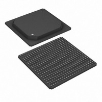
DS32512N# Maxim Integrated Products, DS32512N# Datasheet - Page 85

DS32512N#
Manufacturer Part Number
DS32512N#
Description
IC LIU DS3/E3/STS-1 484-BGA
Manufacturer
Maxim Integrated Products
Type
Line Interface Units (LIUs)r
Datasheet
1.DS32506N.pdf
(130 pages)
Specifications of DS32512N#
Protocol
DS3
Voltage - Supply
3.135 V ~ 3.465 V
Mounting Type
Surface Mount
Package / Case
484-BGA
Lead Free Status / RoHS Status
Lead free / RoHS Compliant
Number Of Drivers/receivers
-
Available stocks
Company
Part Number
Manufacturer
Quantity
Price
Bit 4: Receive Pattern Inversion Control (RPIC) . See Section 8.5.1.
Bit 3: Manual Pattern Resynchronization (MPR). A zero-to-one transition of this bit causes the receive pattern
generator to resynchronize to the incoming pattern. This bit must be changed to zero and back to one for another
resynchronization to be initiated. Note: A manual resynchronization forces the pattern detector out of the “Sync”
state. See Section 8.5.2.
Bit 2: Automatic Pattern Resynchronization Disable (APRD). When APRD = 0, the receive pattern generator
automatically resynchronizes to the incoming pattern if six or more times during the current 64-bit window the
incoming data stream bit and the receive pattern generator output bit did not match. When APRD = 1, the receive
pattern generator does not automatically resynchronize to the incoming pattern. Note: Automatic synchronization is
prevented by not allowing the receive pattern generator to automatically exit the “Sync” state. See Section 8.5.2.
Bit 1: Transmit New Pattern Load (TNPL). A zero-to-one transition of this bit causes the programmed test pattern
(QRSS, PTS, PLF[4:0], PTF[4:0] in the
loaded into the transmit pattern generator. This bit must be changed to zero and back to one for another pattern to
be loaded. Note: The test pattern fields mentioned above must not change for four TCLK cycles after this bit
transitions from zero to one. See Section 8.5.1.
Bit 0: Transmit Pattern Inversion Control (TPIC). See Section 8.5.1.
Register Name:
Register Description:
Register Address:
Bit #
Name
Default
Bit #
Name
Default
Bits 12 to 8: Pattern Tap Feedback (PTF[4:0]). These five bits control the PRBS “tap” feedback of the pattern
generator. The “tap” feedback is from bit y of the pattern generator (y = PTF[4:0] + 1). These bits are ignored when
the BERT block is programmed for a repetitive pattern (PTS = 1). For a PRBS signal, the feedback is an XOR of bit
n and bit y. See Section 8.5.1.
Bit 6: QRSS Enable (QRSS). See Section 8.5.1.
Bit 5: Pattern Type Select (PTS). See Section 8.5.1.
Bits 4 to 0: Pattern Length Feedback (PLF[4:0]). This field controls the “length” feedback of the pattern
generator. The “length” feedback is from bit n of the pattern generator (n = PLF[4:0] + 1). For a PRBS signal, the
feedback is an XOR of bit n and bit y. For a repetitive pattern the feedback is bit n. See Section 8.5.1.
0 = do not invert the incoming data stream
1 = invert the incoming data stream
0 = do not invert the outgoing data stream
1 = invert the outgoing data stream
0 = Disabled: the pattern generator configuration is controlled by PTS, PLF[4:0], PTF[4:0], and
1 = Enabled: the pattern generator configuration is forced to a PRBS pattern with a generating
0 = PRBS pattern
1 = repetitive pattern.
BSP[31:0]
polynomial of x
14 output bits are all zero.
15
—
—
0
7
0
QRSS
20
14
—
0
6
0
+ x
17
BERT.PCR
BERT Pattern Configuration Register
n * 80h + 52h
+ 1, and the output of the pattern generator is forced to one if the next
PTS
13
—
BERT.PCR
0
5
0
85 of 130
register, and BSP[31:0] in the
12
0
4
0
11
0
3
0
PTF[4:0]
PLF[4:0]
10
0
2
0
DS32506/DS32508/DS32512
BERT.SPR
9
0
1
0
registers) to be
8
0
0
0


