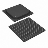
DS32512N# Maxim Integrated Products, DS32512N# Datasheet - Page 35

DS32512N#
Manufacturer Part Number
DS32512N#
Description
IC LIU DS3/E3/STS-1 484-BGA
Manufacturer
Maxim Integrated Products
Type
Line Interface Units (LIUs)r
Datasheet
1.DS32506N.pdf
(130 pages)
Specifications of DS32512N#
Protocol
DS3
Voltage - Supply
3.135 V ~ 3.465 V
Mounting Type
Surface Mount
Package / Case
484-BGA
Lead Free Status / RoHS Status
Lead free / RoHS Compliant
Number Of Drivers/receivers
-
Available stocks
Company
Part Number
Manufacturer
Quantity
Price
Figure 8-6. DS3 and E3 Wander Tolerance
8.3.10 Jitter Transfer
Without the jitter attenuator on the receive side, the receiver attenuates jitter at frequencies above its corner
frequency (approximately 300kHz) and passes jitter at lower frequencies. With the jitter attenuator enabled on the
receive side, the receiver meets the jitter transfer requirements of all applicable telecommunication standards in
Table
8.4 Jitter Attenuator
Each LIU contains an on-board jitter attenuator that can be placed in the receive path or the transmit path or can
be disabled. When only the hardware interface is enabled
pins specify the specify the JA location and buffer depth for all ports. When a microprocessor interface is enabled
(IFSEL
bits specify the JA location and buffer depth for each port individually. The JA buffer depth can be set to 16, 32, 64
or 128 bits.
Figure 8-7
The jitter attenuator consists of a narrowband PLL to retime the selected clock, a FIFO to buffer the associated
data while the clock is being retimed, and logic to prevent FIFO over/underflow in the presence of very large jitter
amplitudes. The JA has a loop bandwidth of reference_clock ÷ 2,058,874 (see corner frequencies in
The JA attenuates jitter at frequencies higher than the loop bandwidth, while allowing jitter (and wander) at lower
frequencies to pass through relatively unaffected.
The jitter attenuator requires a transmission-quality reference clock (i.e., ± 20ppm frequency accuracy and low
jitter). See Section
When the microprocessor interface is enabled, the jitter attenuator indicates the fill status of its FIFO buffer in the
LIU.SRL:JAFL (JA full) and LIU.SRL:JAEL (JA empty) status bits. When the buffer becomes full, the JA
momentarily increases the frequency of the read clock by 6250ppm to avoid buffer overflow and consequent data
errors. When the buffer becomes empty, the JA momentarily decreases the frequency of the read clock by
6250ppm to avoid buffer underflow and consequent data errors. During these momentary frequency adjustments,
jitter is passed through the JA to avoid over/underflow. If the phase noise or frequency offset of the write clock is
large enough to cause the buffer to overflow or underflow, the JA sets both the JAFL bit a n d the JAEL bit to
indicate that data errors have occurred. JAFL and JAEL can cause an interrupt if enabled by the corresponding
enable bits in the
As shown in
in
Table
1-1. See
≠ 000), the
1-1.
also shows the receive jitter transfer when the jitter attenuator is disabled.
Figure 8-7
1000
100
Figure
137.5
10
34.4
805
67
Figure
LIU.SRIE
8.7.1
10
JAS[1:0]
8-7, the jitter attenuator meets the jitter transfer requirements of all applicable standards listed
-5
1.2
8-7.
shows the minimum jitter attenuation for the device when the jitter attenuator is enabled.
for more information about reference clocks and clock selection.
register.
and
6.12
10
JAD[1:0]
-4
pins are ignored, and the LIU.CR1:JAS[1:0] and JAD[1:0] configuration
10
-3
35 of 130
(IFSEL
10
-2
0.032
= 000 and
Frequency (Hz)
10
-1
0.13
HW
Wander Tolerance
= 1), the
G.824 (DS3)
DS32506/DS32508/DS32512
G.823 (E3)
DS325xx
1
1.675
JAS[1:0]
4.4
and
10
Figure
JAD[1:0]
8-7).


