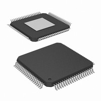
HMP8117CNZ Intersil, HMP8117CNZ Datasheet - Page 12

HMP8117CNZ
Manufacturer Part Number
HMP8117CNZ
Description
IC VIDEO DECODER NTSC/PAL 80PQFP
Manufacturer
Intersil
Type
Video Decoderr
Datasheet
1.HMP8117CNZ.pdf
(45 pages)
Specifications of HMP8117CNZ
Applications
Video
Voltage - Supply, Analog
4.75 V ~ 5.25 V
Voltage - Supply, Digital
4.75 V ~ 5.25 V
Mounting Type
Surface Mount
Package / Case
80-MQFP, 80-PQFP
Lead Free Status / RoHS Status
Lead free / RoHS Compliant
Available stocks
Company
Part Number
Manufacturer
Quantity
Price
NOTES:
Pixel Output Port
Pixel data is output via the P0-P15 pins. Refer to Table 4 for
the output pin definition as a function of the output mode.
Refer to the section “CYCLE SLIPPING AND REAL-TIME
PIXEL JITTER” for PLL and interface considerations.
8-Bit YCbCr Output
Each YCbCr data byte is output following each rising edge of
CLK2. The YCbCr data is multiplexed as [Cb Y Cr Y′ Cb Y
NOTE:
16-Bit YCbCr, 15-Bit RGB, or 16-RGB Output
For 16-bit YCbCr, 15-bit RGB data, or 16-bit RGB output
modes, the data is output following the rising edge of CLK2
with DVALID asserted. Either linear or gamma-corrected
RGB data may be output. The pixel output timing is shown in
Figures 10 to 13.
BLANK, HSYNC, VSYNC, DVALID, VBIVALID, and FIELD
are output following the rising edge of CLK2. When BLANK
7. Y
8. When DVLD_LTC is set to 1, the polarity of DVALID needs to be set to active low, otherwise DVALID will stay low during active video and be
6. Y
cycle due to the 4:2:2 subsampling. Pixel data is not output during the blanking period, but the values are forced to blanking levels.
gated with the clock only during the blanking interval.
cycle due to the 4:2:2 subsampling. Pixel data is not output during the blanking period, but the values are forced to blanking levels.
0
0
BLANK
DVALID
P[15-8]
is the first active luminance pixel data of a line. Cb
is the first active luminance pixel data of a line. Cb
DVALID
BLANK
CLK
P[15-8]
CLK
12
t
DVLD
FIGURE 9. OUTPUT TIMING FOR 8-BIT YCbCr MODE (DVLD_LTC = 1)
FIGURE 8. OUTPUT TIMING FOR 8-BIT YCbCr MODE (DVLD_LTC = 0)
t
DVLD
Cb
Cb
0
0
Y
0
Y
0
0
0
and Cr
and Cr
Cr
0
Cr
HMP8117
0
0
are first active chrominance pixel data in a line. Cb and Cr will alternate every
are first active chrominance pixel data in a line. Cb and Cr will alternate every
0
Y
1
Y
1
Cr Y′...], with the first active data each scan line containing
Cb data. The pixel output timing is shown in Figures 8 and 9.
BLANK, HSYNC, VSYNC, DVALID, VBIVALID, and FIELD
are output following the rising edge of CLK2. When BLANK
is asserted and VBIVALID is deasserted, the YCbCr outputs
have a value of 16 for Y and 128 for Cb and Cr. The behavior
of the DVALID output is determined by bit 4 (DVLD_LTC) of
the GENLOCK CONTROL register 04
is asserted and VBIVALID is deasserted, the YCbCr outputs
have a value of 16 for Y and 128 for Cb and Cr; the RGB
outputs have a value of 0.
The behavior of the DVALID output is determined by bit 4
(DVLD_LTC) and bit 5 (DLVD_DCYC) of the GENLOCK
CONTROL register 04
Cb
Cb
2
2
Y
2
Y
2
Cr
H
2
.
Cr
2
Y
3
Y
3
H
.
Cb
Cb
4
4
Y
Y
April 19, 2007
4
4
FN4643.3


