HMP8117CNZ Intersil, HMP8117CNZ Datasheet - Page 20
HMP8117CNZ
Manufacturer Part Number
HMP8117CNZ
Description
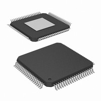
IC VIDEO DECODER NTSC/PAL 80PQFP
Manufacturer
Intersil
Type
Video Decoderr
Datasheet
1.HMP8117CNZ.pdf
(45 pages)
Specifications of HMP8117CNZ
Applications
Video
Voltage - Supply, Analog
4.75 V ~ 5.25 V
Voltage - Supply, Digital
4.75 V ~ 5.25 V
Mounting Type
Surface Mount
Package / Case
80-MQFP, 80-PQFP
Lead Free Status / RoHS Status
Lead free / RoHS Compliant
Available stocks
Company
Part Number
Manufacturer
Quantity
Price


During PAL (B, D, G, H, I, N, N
line of VBI data are lines 6 and 318, and the last possible
NOTES:
During PAL (M) operation, the first possible line of VBI data
is lines 7 and 269, and the last possible lines are the last
blanked scan lines. Lines 523-6 and 261-268 are always
blanked.
Real Time Control Interface
The Real Time Control Interface (RTCI) outputs timing
information for a NTSC/PAL encoder as BT.656 ancillary
data. This allows the encoder to generate “clean” output
video.
RTCI information via BT.656 ancillary data is shown in Table
9. If enabled, this transfer occurs once per line and is
completed before the start of the SAV sequence.
The PSW bit is always a “0” for NTSC encoding. During PAL
encoding, it indicates the sign of V (“0” = negative;
“1” = positive) for that scan line.
Host Interface
All internal registers may be written to or read by the host
processor at any time, except for those bits identified as
read-only. The bit descriptions for the control registers are
listed beginning with Table 10.
The HMP8117 supports the fast-mode (up to 400kbps) I
interface consisting of the SDA and SCL pins. The device
39. ep = even parity for P8-P13.
40. CRC = Sum of P8-P14 of Data ID through last user data word. Preset to all zeros, carry is ignored.
Data Block Number
Data Word Count
PIXEL INPUT
Increment
Increment
Preamble
FSCPLL
Data ID
HPLL
CRC
20
C
) operation, the first possible
TABLE 9. OUTPUTTING RTCI AS BT.656 ANCILLARY DATA
P15
P14
P14
P14
P14
P14
P14
P14
P14
P14
P14
P14
P14
0
1
1
bit 6
P14
ep
ep
ep
ep
ep
ep
ep
ep
ep
ep
ep
0
1
1
2
C
HMP8117
F2 = 0
PSW
P13
bit 5
0
1
1
1
0
0
0
0
0
0
0
0
lines are the last blanked scan lines. Lines 623-5 and 311-
317 are always blanked.
acts as a slave for receiving and transmitting data over the
serial interface. When the interface is not active, SCL and
SDA must be pulled high using external 4kΩ pull-up
resistors. The SA input pin determines the slave address for
the HMP8117. If the SA pin is pulled low, the address is
1000100x
up resistor, the address is 1000101x
address is the I
Data is placed on the SDA line when the SCL line is low and
held stable when the SCL line is pulled high. Changing the
state of the SDA line while SCL is high will be interpreted as
either an I
Figure 18.
During I
address is treated as the control register sub address and is
written into the internal address register. Any remaining data
bytes sent during an I
registers, beginning with the register specified by the
address register as given in the first byte. The address
register is then auto-incremented after each additional data
byte sent on the I
reserved bits within registers or reserved registers are
ignored.
F1 = 0
P12
bit 4
0
0
0
1
1
1
0
0
0
0
0
0
0
2
C write cycles, the first data byte after the slave
B
2
C bus START or STOP condition as indicated by
:
. If the SA pin is pulled high through a 10kΩ pull-
2
C read flag.)
bit 31
bit 27
bit 7
bit 3
bit 3
2
P11
C bus during a write cycle. Writes to
0
1
1
0
0
0
0
0
0
0
2
C write cycle are written to the control
bit 30
bit 26
bit 6
bit 2
bit 2
P10
0
1
1
1
0
0
0
0
0
0
B
. (This ‘x’ bit in the
bit 29
bit 25
bit 5
bit 1
bit 1
P9
0
1
1
0
0
1
0
0
0
0
April 19, 2007
bit 28
bit 24
bit 4
bit 0
bit 0
P8
FN4643.3
0
1
1
1
1
1
0
0
0
0
Related parts for HMP8117CNZ
Image
Part Number
Description
Manufacturer
Datasheet
Request
R

Part Number:
Description:
Ntsc/pal Video Decoder
Manufacturer:
Intersil Corporation
Datasheet:
Part Number:
Description:
Intersil Corporation [CMOS Serial Controller Interface]
Manufacturer:
Intersil Corporation
Datasheet:
Part Number:
Description:
Manufacturer:
Intersil Corporation
Datasheet:
Part Number:
Description:
357-036-542-201 CARDEDGE 36POS DL .156 BLK LOPRO
Manufacturer:
Intersil Corporation
Datasheet:
Part Number:
Description:
1024-Word x 4-Bit LSI Static RAM
Manufacturer:
Intersil Corporation
Datasheet:
Part Number:
Description:
General Purpose NPN Transistor Arrays FN341.4
Manufacturer:
Intersil Corporation
Datasheet:
Part Number:
Description:
CMOS 16-Bit Microprocessor
Manufacturer:
Intersil Corporation
Datasheet:
Part Number:
Description:
Manufacturer:
Intersil Corporation
Datasheet:
Part Number:
Description:
Manufacturer:
Intersil Corporation
Datasheet:
Part Number:
Description:
Manufacturer:
Intersil Corporation
Datasheet:
Part Number:
Description:
Manufacturer:
Intersil Corporation
Datasheet:
Part Number:
Description:
CMOS 6-Bit Latch and Decoder Memory Interfaces
Manufacturer:
Intersil Corporation
Datasheet:
Part Number:
Description:
CA3046General Purpose NPN Transistor Arrays
Manufacturer:
Intersil Corporation
Datasheet:
Part Number:
Description:
Manufacturer:
Intersil Corporation
Datasheet:
Part Number:
Description:
TR909 DLC/FLC SLIC with Low Power Standby
Manufacturer:
Intersil Corporation
Datasheet: