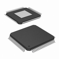
HMP8117CNZ Intersil, HMP8117CNZ Datasheet - Page 40

HMP8117CNZ
Manufacturer Part Number
HMP8117CNZ
Description
IC VIDEO DECODER NTSC/PAL 80PQFP
Manufacturer
Intersil
Type
Video Decoderr
Datasheet
1.HMP8117CNZ.pdf
(45 pages)
Specifications of HMP8117CNZ
Applications
Video
Voltage - Supply, Analog
4.75 V ~ 5.25 V
Voltage - Supply, Digital
4.75 V ~ 5.25 V
Mounting Type
Surface Mount
Package / Case
80-MQFP, 80-PQFP
Lead Free Status / RoHS Status
Lead free / RoHS Compliant
Available stocks
Company
Part Number
Manufacturer
Quantity
Price
Applications Information
Direct Interface to Video Encoders
Direct interface to a video encoder will induce pixel jitter in
the output video and is therefore not recommended as a
primary data interface. The jitter will occur with all decoder
output formats, including BT.656. However, pixel jitter may
be acceptable for some applications; such as a “preview
mode” prior to image capture or compression. For more
detail, reference“Cycle Slipping and Real-Time Pixel Jitter”
on page 7.
Decoder Upgrades
The following table describe the impacts to pins for
upgrading from the HMP8112/A or HMP8115 to the
HMP8117.
Typical Programming Sequence
The following pseudo code provides a typical programming
sequence to initialize the HMP8117 using the default 16-bit
YCbCr output data format.
SetReg 0x1F = 0x80 // Soft Reset
SetReg 0x37 = 0x90 // Wider HSYNC Detect Window
SetReg 0x42 = 0x30 // Recommended Value
SetReg 0x50 = 0x21 // Slower PFG
SetReg 0x52 = 0x22 // Recommended Value
SetReg 0x53 = 0xF0 // Large AGC Hysteresis
SetReg 0x03 = 0xC0 // Enable Data/Timing Outputs
PCB Layout Considerations
A PCB board with a minimum of 4 layers is recommended,
with layers 1 and 4 (top and bottom) for signals and layers
2 and 3 for power and ground. The PCB layout should
28
78
29
76
9,8,19
27
44
61
13
30, 32,
73, 77
Pin #
TABLE 67. UPGRADING FROM HMP8112/A OR HMP8115
GAIN_CNTL
(Now RSET)
DEC_T
(Now REF_CAP)
CCLAMP_CAP
(Now CCAP)
LCLAMP_CAP
(Now LCAP)
L_OUT,
L_ADIN, and C
WPE
(Now SA)
DVCC/NC
(Now INTREQ)
DGND/NC
(Now VBIVALID)
CLK2
(Now NC)
DEC_L, DGND,
DGND, AGC_CAP
HMP8112/15 Pin
Use single 12.1k resistor to AGND.
Remove any decoupling caps.
Change to single 1.0uF capacitor
(1206-size XR7-type) to AGND.
Change to 0.1uF capacitor.
Change to 0.1uF capacitor.
Recommend use of new anti-alias
filter from Reference Schematic.
Pull low for I2C address compatibility
with HMP8112/A.
Pin actually NC on HMP8112/A.
Float or use 10K pullup to VCC.
Pin actually NC on HMP8112/A.
Float or use 10K pullup to VCC.
Trace may be deleted to reduce
reflections on CLK2 at pin 38.
Pins no longer used (NC). Capacitors
used at these pins may be removed.
40
HMP8117 Impact
HMP8117
implement the lowest possible noise on the power and
ground planes by providing excellent decoupling. The
optimum layout places the HMP8117 as close as possible
to the power supply connector and the video input
connector. Place external components as close as possible
to the appropriate pin using short, wide traces.
ANALOG POWER PLANE
The analog power plane (V
separate from the common board digital power plane (V
with a gap between the two planes of at least 1/8 inch. The
V
point though a low-resistance ferrite bead, such as a
Ferroxcube 5659065-3B, Fair-Rite 2743001111, or TDK
BF45-4001. The ferrite bead provides resistance to
switching currents, improving the performance of HMP8117.
If a separate linear regulator is used to provide power to the
analog power plane, the power-up sequence should be
designed to ensure latch up will not occur. A separate linear
regulator is recommended if the power supply noise on the V
pins exceeds 200mV.
ANALOG GROUND PLANE
A separate analog ground (AGND) plane is recommended
with a single point connection to the digital ground (GND)
plane using a ferrite bead as mentioned above.
POWER SUPPLY DECOUPLING
Decouple each V
plane using a 0.1μF ceramic chip capacitor. Bulk decouple
the power planes using a 1.0μF ceramic chip capacitor
located at each corner of the device. (One capacitor placed
at the top left corner for V
the other corners for V
capacitor for the analog power plane may also be used to
control excessive low-frequency power supply ripple. See
Figure 20, HMP8117 Reference Schematics.
ANALOG SIGNALS
Traces containing digital signals should not be routed over,
under, or adjacent to the analog output traces to minimize
cross-talk. If this is not possible, coupling can be minimized
by routing the digital signals at a 90 degree angle to the
analog signals. The analog traces should also not overlay
the V
supply rejection.
Evaluation Board
HMPVIDEVAL/ISA
The HMPVIDEVAL/ISA board provides a complete video
frame-grabber platform to evaluate all modes of the video
decoder and encoder. The ISA style PC add-in board
supports a complete Windows 95 software application to
easily operate all features of the evaluation platform.
AA
plane should be connected to the V
CC
power plane to maximize high-frequency power
AA
and V
CC
AA
.) A single 47μF decoupling
CC
AA
and three capacitors placed at
) is recommended to be
pin to the appropriate ground
CC
plane at a single
April 19, 2007
FN4643.3
CC
AA
)


