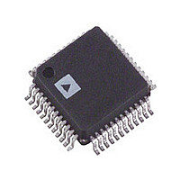
AD9847AKST Analog Devices Inc, AD9847AKST Datasheet - Page 15

AD9847AKST
Manufacturer Part Number
AD9847AKST
Description
IC CCD SIGNAL PROC 10BIT 48-LQFP
Manufacturer
Analog Devices Inc
Type
CCD Signal Processor, 10-Bitr
Datasheet
1.AD9847AKSTZRL.pdf
(28 pages)
Specifications of AD9847AKST
Rohs Status
RoHS non-compliant
Input Type
Logic
Output Type
Logic
Interface
3-Wire Serial
Mounting Type
Surface Mount
Package / Case
48-LQFP
Analog Front End Type
CCD
Analog Front End Category
Video
Interface Type
Serial (3-Wire)
Sample Rate
40MSPS
Input Voltage Range
0.5V
Operating Supply Voltage (min)
2.7/3V
Operating Supply Voltage (typ)
3.3/5V
Operating Supply Voltage (max)
3.6/5.5V
Resolution
10b
Number Of Adc's
1
Power Supply Type
Analog/Digital
Operating Temp Range
-20C to 85C
Operating Temperature Classification
Commercial
Mounting
Surface Mount
Pin Count
48
Package Type
LQFP
Number Of Channels
1
Current - Supply
-
Lead Free Status / RoHS Status
Not Compliant
Available stocks
Company
Part Number
Manufacturer
Quantity
Price
Company:
Part Number:
AD9847AKST
Manufacturer:
AD
Quantity:
1 831
Company:
Part Number:
AD9847AKST
Manufacturer:
ADI
Quantity:
244
Part Number:
AD9847AKST
Manufacturer:
ADI/亚德诺
Quantity:
20 000
Company:
Part Number:
AD9847AKSTZ
Manufacturer:
Analog Devices Inc
Quantity:
10 000
Company:
Part Number:
AD9847AKSTZRL
Manufacturer:
Analog Devices Inc
Quantity:
10 000
REV. A
Address
AFE Register Breakdown
oprmode
ctlmode
PRECISION TIMING HIGH SPEED TIMING
GENERATION
The AD9847 generates flexible high speed timing signals using
the Precision Timing core. This core is the foundation for generating
the timing used for both the CCD and the AFE, the reset gate RG,
horizontal drivers H1–H4, and the SHP/SHD sample clocks.
A unique architecture makes it routine for the system designer to
optimize image quality by providing precise control over the hori-
zontal CCD readout and the AFE correlated double sampling.
Bit
Content
[7:0]
[1:0]
[2]
[3]
[4]
[5]
[6]
[7]
[5:0]
[2:0]
[3]
[4]
[5]
POSITION
PERIOD
1 PIXEL
NOTES
1. PIXEL CLOCK PERIOD IS DIVIDED INTO 48 POSITIONS, PROVIDING FINE EDGE RESOLUTION FOR HIGH SPEED CLOCKS.
2. THERE IS A FIXED DELAY FROM THE CLI INPUT TO THE INTERNAL PIXEL PERIOD POSITIONS (
CLI
t
CLIDLY
Figure 4. High Speed Clock Resolution from CLI Master Clock Input
Width
2'h0
2'h1
2'h2
2'h3
3'h0
3'h1
3'h2
3'h3
3'h4
3'h5
3'h6
3'h7
1'h0
1'h1
1'h0
1'h1
P[0]
Default
Value
8'h0
6'h0
...
P[12]
Register Name
powerdown[1:0]
disblack
test mode
test mode
test mode
test mode
test mode
ctlmode[2:0]
enablepxga
outputlat
tristateout
–15–
Timing Resolution
The Precision Timing core uses a 1
a reference. This clock should be the same as the CCD pixel clock
frequency. Figure 4 illustrates how the internal timing core
divides the master clock period into 48 steps or edge positions.
Therefore, the edge resolution of the Precision Timing core is
(t
Applications Information section.
CLI
P[24]
/48). For more information on using the CLI input, see the
Register Description
8'h00 {oprmode[5:0]}, 8'h01 {oprmode[7:6]}
Full Power
Disable Black Loop Clamping (High Active)
Serial Address: 8'h06 {cltmode[5:0]}
Enable PxGA (High Active)
Latch Output Data on Selected DOUT Edge
ADC Outputs Are Driven
Serial Address:
Fast Recovery
Reference Standby
Total Shutdown
Test Mode—Should Be Set Low
Test Mode—Should Be Set High
Test Mode—Should Be Set Low
Test Mode—Should Be Set Low
Test Mode—Should Be Set Low
Off
Mosaic Separate
VD Selected/Mosaic Interlaced
Mosaic Repeat
Three-Color
Three-Color II
Four-Color
Four-Color II
Leave Output Latch Transparent
ADC Outputs Are Three-Stated
P[36]
t
CLIDLY
= 6 ns TYP).
master clock input (CLI) as
...
P[48]=P[0]
AD9847


