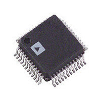
AD9847AKST Analog Devices Inc, AD9847AKST Datasheet - Page 8

AD9847AKST
Manufacturer Part Number
AD9847AKST
Description
IC CCD SIGNAL PROC 10BIT 48-LQFP
Manufacturer
Analog Devices Inc
Type
CCD Signal Processor, 10-Bitr
Datasheet
1.AD9847AKSTZRL.pdf
(28 pages)
Specifications of AD9847AKST
Rohs Status
RoHS non-compliant
Input Type
Logic
Output Type
Logic
Interface
3-Wire Serial
Mounting Type
Surface Mount
Package / Case
48-LQFP
Analog Front End Type
CCD
Analog Front End Category
Video
Interface Type
Serial (3-Wire)
Sample Rate
40MSPS
Input Voltage Range
0.5V
Operating Supply Voltage (min)
2.7/3V
Operating Supply Voltage (typ)
3.3/5V
Operating Supply Voltage (max)
3.6/5.5V
Resolution
10b
Number Of Adc's
1
Power Supply Type
Analog/Digital
Operating Temp Range
-20C to 85C
Operating Temperature Classification
Commercial
Mounting
Surface Mount
Pin Count
48
Package Type
LQFP
Number Of Channels
1
Current - Supply
-
Lead Free Status / RoHS Status
Not Compliant
Available stocks
Company
Part Number
Manufacturer
Quantity
Price
Company:
Part Number:
AD9847AKST
Manufacturer:
AD
Quantity:
1 831
Company:
Part Number:
AD9847AKST
Manufacturer:
ADI
Quantity:
244
Part Number:
AD9847AKST
Manufacturer:
ADI/亚德诺
Quantity:
20 000
Company:
Part Number:
AD9847AKSTZ
Manufacturer:
Analog Devices Inc
Quantity:
10 000
Company:
Part Number:
AD9847AKSTZRL
Manufacturer:
Analog Devices Inc
Quantity:
10 000
AD9847
SYSTEM OVERVIEW
Figures 1a and 1b show the typical system application diagrams
for the AD9847. The CCD output is processed by the AD9847’s
AFE circuitry, which consists of a CDS, PxGA, VGA, black
level clamp, and A/D converter. The digitized pixel information is
sent to the digital image processor chip, where all post-processing
and compression occurs. To operate the CCD, CCD timing param-
eters are programmed into the AD9847 from the image processor
through the 3-wire serial interface. From the system master clock,
CLI, provided by the image processor, the AD9847 generates
the high speed CCD clocks and all internal AFE clocks. All
AD9847 clocks are synchronized with VD and HD.
Figure 1a shows the AD9847 used in internal mode, in which all
the horizontal pulses (CLPOB, CLPDM, PBLK, and HBLK)
are programmed and generated internally. Figure 1b shows the
AD9847 operating in external mode, in which the horizontal
pulses are supplied externally by the image processor.
The H-drivers for H1–H4 and RG are included in the AD9847,
allowing these clocks to be directly connected to the CCD. The
AD9847 supports H-drive voltage of 5 V.
CCD
Figure 1a. Typical Application (Internal Mode)
H1–H4, RG
V-DRIVER
CCDIN
INTERFACE
SERIAL
INTEGRATED
AD9847
AFE + TD
V1–V4, VSG1–VSG8, SUBCK
HD, VD
DOUT
CLI
DIGITAL IMAGE
PROCESSING
ASIC
–8–
Figure 2 shows the horizontal and vertical counter dimensions for
the AD9847. All internal horizontal clocking is programmed using
these dimensions to specify line and pixel locations.
Figure 1b. Typical Application (External Mode)
CCD
Figure 2. Vertical and Horizontal Counters
V-DRIVER
H1–H4, RG
CCDIN
12-BIT HORIZONTAL = 4096 PIXELS MAX
12-BIT VERTICAL = 4096 LINES MAX
MAXIMUM FIELD DIMENSIONS
INTERFACE
SERIAL
INTEGRATED
AD9847
AFE + TD
V1–V4, VSG1–VSG8, SUBCK
CLPDM
CLPOB
HD, VD
DOUT
HBLK
PBLK
CLI
DIGITAL IMAGE
PROCESSING
ASIC
REV. A


