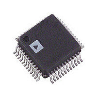
AD9847AKST Analog Devices Inc, AD9847AKST Datasheet - Page 26

AD9847AKST
Manufacturer Part Number
AD9847AKST
Description
IC CCD SIGNAL PROC 10BIT 48-LQFP
Manufacturer
Analog Devices Inc
Type
CCD Signal Processor, 10-Bitr
Datasheet
1.AD9847AKSTZRL.pdf
(28 pages)
Specifications of AD9847AKST
Rohs Status
RoHS non-compliant
Input Type
Logic
Output Type
Logic
Interface
3-Wire Serial
Mounting Type
Surface Mount
Package / Case
48-LQFP
Analog Front End Type
CCD
Analog Front End Category
Video
Interface Type
Serial (3-Wire)
Sample Rate
40MSPS
Input Voltage Range
0.5V
Operating Supply Voltage (min)
2.7/3V
Operating Supply Voltage (typ)
3.3/5V
Operating Supply Voltage (max)
3.6/5.5V
Resolution
10b
Number Of Adc's
1
Power Supply Type
Analog/Digital
Operating Temp Range
-20C to 85C
Operating Temperature Classification
Commercial
Mounting
Surface Mount
Pin Count
48
Package Type
LQFP
Number Of Channels
1
Current - Supply
-
Lead Free Status / RoHS Status
Not Compliant
Available stocks
Company
Part Number
Manufacturer
Quantity
Price
Company:
Part Number:
AD9847AKST
Manufacturer:
AD
Quantity:
1 831
Company:
Part Number:
AD9847AKST
Manufacturer:
ADI
Quantity:
244
Part Number:
AD9847AKST
Manufacturer:
ADI/亚德诺
Quantity:
20 000
Company:
Part Number:
AD9847AKSTZ
Manufacturer:
Analog Devices Inc
Quantity:
10 000
Company:
Part Number:
AD9847AKSTZRL
Manufacturer:
Analog Devices Inc
Quantity:
10 000
AD9847
Driving the CLI Input
The AD9847’s master clock input (CLI) may be used in two
different configurations, depending on the application. Figure 23a
shows a typical dc-coupled input from the master clock source.
When the dc-coupled technique is used, the master clock signal
should be at standard 3 V CMOS logic levels. As shown in
Figure 23b, a 1000 pF ac-coupling capacitor may be used between
the clock source and the CLI input. In this configuration, the CLI
input will self-bias to the proper dc voltage level of approximately
1.4 V. When the ac-coupled technique is used, the master clock
signal can be as low as ± 500 mV in amplitude.
H3
17
H1
13
Figure 22a. CCD Connections (2 H-Clock)
Figure 22b. CCD Connections (4 H-Clock)
Figure 23a. CLI Connection, DC-Coupled
18
H4
H2
AD9847
AD9847
14
AD9847
H1
13
H1
H3
17
H1
H2
14
H2
H4
18
H2
CCD IMAGER
RG
CCD IMAGER
CLI
RG
20
RG
23
RG
20
SIGNAL
OUT
29
SIGNAL
CCDIN
H2
OUT
29
CCDIN
H1
ASIC
MASTER
CLOCK
–26–
Internal Mode Circuit Configuration
The AD9847 may be used in internal mode using the circuit
configuration of Figure 24. Internal mode uses the same circuit as
Figure 21, except that the horizontal pulses (CLPOB, CLPDM,
PBLK, and HBLK) are internally generated in the AD9847.
These pins may be grounded when internal mode is used. Only
the HD and VD signals are required from the ASIC.
TIMING EXAMPLES FOR DIFFERENT SEQUENCES
28
V
Figure 24. Internal Mode Circuit Configuration
4
Figure 23b. CLI Connection, AC-Coupled
AD9847
44
AD9847
43
H
Figure 25. Typical CCD
42
41
CLI
23
40
48
39
1nF
2
10
SEQUENCE 2
SEQUENCE 3
SEQUENCE 2
2
LPF
HD/VD
INPUTS
MASTER
CLOCK
ASIC
REV. A


