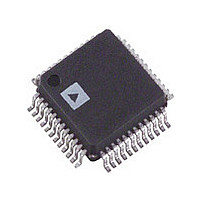
AD9847AKST Analog Devices Inc, AD9847AKST Datasheet - Page 16

AD9847AKST
Manufacturer Part Number
AD9847AKST
Description
IC CCD SIGNAL PROC 10BIT 48-LQFP
Manufacturer
Analog Devices Inc
Type
CCD Signal Processor, 10-Bitr
Datasheet
1.AD9847AKSTZRL.pdf
(28 pages)
Specifications of AD9847AKST
Rohs Status
RoHS non-compliant
Input Type
Logic
Output Type
Logic
Interface
3-Wire Serial
Mounting Type
Surface Mount
Package / Case
48-LQFP
Analog Front End Type
CCD
Analog Front End Category
Video
Interface Type
Serial (3-Wire)
Sample Rate
40MSPS
Input Voltage Range
0.5V
Operating Supply Voltage (min)
2.7/3V
Operating Supply Voltage (typ)
3.3/5V
Operating Supply Voltage (max)
3.6/5.5V
Resolution
10b
Number Of Adc's
1
Power Supply Type
Analog/Digital
Operating Temp Range
-20C to 85C
Operating Temperature Classification
Commercial
Mounting
Surface Mount
Pin Count
48
Package Type
LQFP
Number Of Channels
1
Current - Supply
-
Lead Free Status / RoHS Status
Not Compliant
Available stocks
Company
Part Number
Manufacturer
Quantity
Price
Company:
Part Number:
AD9847AKST
Manufacturer:
AD
Quantity:
1 831
Company:
Part Number:
AD9847AKST
Manufacturer:
ADI
Quantity:
244
Part Number:
AD9847AKST
Manufacturer:
ADI/亚德诺
Quantity:
20 000
Company:
Part Number:
AD9847AKSTZ
Manufacturer:
Analog Devices Inc
Quantity:
10 000
Company:
Part Number:
AD9847AKSTZRL
Manufacturer:
Analog Devices Inc
Quantity:
10 000
AD9847
High Speed Clock Programmability
Figure 5 shows how the high speed clocks RG, H1–H4, SHP,
and SHD are generated. The RG pulse has programmable rising
and falling edges and may be inverted using the polarity control.
The horizontal clocks H1 and H3 have programmable rising and
falling edges and polarity control. The H2 and H4 clocks are
always inverses of H1 and H3, respectively. Table II summarizes
the high speed timing registers and their parameters.
Register Name
POL
POSLOC
NEGLOC
DRV
Quadrant
I
II
III
IV
CCD SIGNAL
Edge Location (Decimal)
0 to 11
12 to 23
24 to 35
36 to 47
6b
6b
3b
Length
1b
H1/H3
H2/H4
RG
NOTES
PROGRAMMABLE CLOCK POSITIONS:
(1) RG RISING EDGE AND (2) FALLING EDGE
(3) SHP AND (4) SHD SAMPLE LOCATION
(5) H1/H3 RISING EDGE POSITION AND (6) FALLING EDGE POSITION (H2/H4 ARE INVERSE OF H1/H3)
(5)
(1)
0–47 Edge Location
0–47 Edge Location
0–7 Current Steps
Range
High/Low
(2)
Figure 5. High Speed Clock Programmable Locations
Table II. H1–H4, RG, SHP, SHD Timing Parameters
(3)
Table III. Precision Timing Edge Locations
(6)
(4)
Register Value (Decimal)
0 to 11
16 to 27
32 to 43
48 to 59
Polarity Control for H1, H3, and RG (0 = No Inversion, 1 = Inversion)
Positive Edge Location for H1, H3, and RG
Sample Location for SHP, SHD
Negative Edge Location for H1, H3, and RG
Drive Current for H1–H4 and RG Outputs (3.5 mA per Step)
Description
–16–
The edge location registers are 6 bits wide, but there are only 48
valid edge locations available. Therefore, the register values are
mapped into four quadrants, with each quadrant containing 12 edge
locations. Table III shows the correct register values for the
corresponding edge locations. Figure 6 shows the range and
default locations of the high speed clock signals.
Register Value (Binary)
000000 to 001011
010000 to 011011
100000 to 101011
110000 to 111011
REV. A


