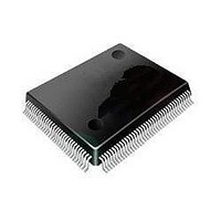
STM32F407VGT6 STMicroelectronics, STM32F407VGT6 Datasheet - Page 72

STM32F407VGT6
Manufacturer Part Number
STM32F407VGT6
Description
IC MCU 32BIT 1MB FLASH 100LQFP
Manufacturer
STMicroelectronics
Specifications of STM32F407VGT6
Core Processor
ARM Cortex-M4
Core Size
32-Bit
Speed
168MHz
Connectivity
CAN, I²C, IrDA, LIN, SPI, UART/USART, USB OTG
Peripherals
Brown-out Detect/Reset, DMA, I²S, POR, PWM, WDT
Number Of I /o
82
Program Memory Size
1MB (1M x 8)
Program Memory Type
FLASH
Eeprom Size
-
Ram Size
192K x 8
Voltage - Supply (vcc/vdd)
1.8 V ~ 3.6 V
Data Converters
A/D 16x12b, D/A 2x12b
Oscillator Type
Internal
Operating Temperature
-40°C ~ 85°C
Package / Case
*
Core
ARM Cortex M4
Processor Series
STM32F4
Data Bus Width
32 bit
Maximum Clock Frequency
168 MHz
Data Ram Size
192 KB
On-chip Adc
Yes
Number Of Programmable I/os
82
Number Of Timers
10
Operating Supply Voltage
1.7 V to 3.6 V
Mounting Style
SMD/SMT
A/d Bit Size
12 bit
A/d Channels Available
16
Interface Type
CAN, I2C, I2S, SPI, UART
Lead Free Status / Rohs Status
Lead free / RoHS Compliant
Other names
497-11605
Available stocks
Company
Part Number
Manufacturer
Quantity
Price
Company:
Part Number:
STM32F407VGT6
Manufacturer:
MXIC
Quantity:
1 459
Company:
Part Number:
STM32F407VGT6
Manufacturer:
STMicroelectronics
Quantity:
10 000
Part Number:
STM32F407VGT6TR
Manufacturer:
ST
Quantity:
20 000
Electrical characteristics
5.3.7
Table 24.
1. Based on characterization, not tested in production.
2. The wakeup times are measured from the wakeup event to the point in which the application code reads the first instruction.
3. t
72/154
t
WUSTDBY
WUSTDBY
t
t
WUSLEEP
WUSTOP
Symbol
minimum and maximum values are given at 105 °C and –45 °C, respectively.
(2)(3)
(2)
(2)
Table 23.
1. TBD stands for “to be defined”.
2. External clock is 25 MHz (HSE oscillator with 25 MHz crystal) and PLL is on.
3. EN1 bit is set in DAC_CR register.
4. EN2 bit is set in DAC_CR register.
5. f
Wakeup time from low-power mode
The wakeup times given in
oscillator. The clock source used to wake up the device depends from the current operating
mode:
●
●
All timings are derived from tests performed under ambient temperature and V
voltage conditions summarized in
Low-power mode wakeup timings
APB2
ADC
Stop or Standby mode: the clock source is the RC oscillator
Sleep mode: the clock source is the clock that was set before entering Sleep mode.
Wakeup from Sleep mode
Wakeup from Stop mode (regulator in Run mode)
Wakeup from Stop mode (regulator in low power mode)
Wakeup from Stop mode (regulator in low power mode
and Flash memory in Deep power down mode)
Wakeup from Standby mode
= f
PCLK2
Peripheral current consumption
/2, ADON bit set in ADC_CR2 register.
Peripheral
SDIO
TIM1
TIM8
TIM9
TIM10
TIM11
ADC1
ADC2
ADC3
SPI1
USART1
USART6
(5)
(5)
(5)
(2)
Table 24
Parameter
Doc ID 022152 Rev 1
Table
is measured on a wakeup phase with a 16 MHz HSI RC
10.
(1)
Typical consumption at 25 °C
(continued)
TBD
TBD
TBD
TBD
TBD
TBD
TBD
TBD
TBD
TBD
TBD
TBD
Min
STM32F405xx, STM32F407xx
260
-
-
-
-
(1)
Typ
110
375
13
17
1
(1)
Max
DD
480
40
-
-
-
(1)
supply
Unit
mA
Unit
µs
µs
µs


