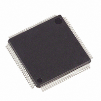
DS21Q50L Maxim Integrated Products, DS21Q50L Datasheet - Page 20

DS21Q50L
Manufacturer Part Number
DS21Q50L
Description
IC TRANSCEIVER E1 QUAD 100-LQFP
Manufacturer
Maxim Integrated Products
Datasheet
1.DS21Q50L.pdf
(87 pages)
Specifications of DS21Q50L
Function
Transceiver
Interface
E1
Number Of Circuits
4
Voltage - Supply
3.14 V ~ 3.47 V
Current - Supply
230mA
Operating Temperature
0°C ~ 70°C
Mounting Type
Surface Mount
Package / Case
100-LQFP
Includes
AIS Alarms Detector and Generator, Loopback Functions, PRBS Generator / Detector, Remote Detector and Generator
Lead Free Status / RoHS Status
Contains lead / RoHS non-compliant
Power (watts)
-
Available stocks
Company
Part Number
Manufacturer
Quantity
Price
Part Number:
DS21Q50L
Manufacturer:
MAXIM/美信
Quantity:
20 000
Company:
Part Number:
DS21Q50L+
Manufacturer:
SPANSION
Quantity:
119
Company:
Part Number:
DS21Q50L+
Manufacturer:
MAXIM
Quantity:
3
Company:
Part Number:
DS21Q50L-W+
Manufacturer:
Maxim Integrated
Quantity:
10 000
3. HOST INTERFACE PORT
The DS21Q50 is controlled either through a nonmultiplexed bus, a multiplexed bus, or serial interface
bus by an external microcontroller or microprocessor. The device can operate with either Intel or
Motorola bus timing configurations. See
Motorola bus signals are listed in parentheses (). See Functional Timing Diagrams in Section
details.
Table 3-1. Bus Mode Select
3.1 Parallel Port Operation
When using the parallel interface on the DS21Q50 (BTS1 = 0) the user has the option for either
multiplexed bus operation (BTS1 = 0, BTS0 = 0) or nonmultiplexed bus operation (BTS1 = 0, BTS0 = 1).
The DS21Q50 can operate with either Intel or Motorola bus timing configurations. If the PBTS pin is
wired low, Intel timing is selected; if wired high, Motorola timing is selected. All Motorola bus signals
are listed in parentheses (). See the timing diagrams in AC Timing Parameters and Diagrams in
Section
3.2 Serial Port Operation
Setting BTS1 pin = 1 and the BTS0 pin = 0 enables the serial bus interface on the DS21Q50. Port
read/write timing is unrelated to the system transmit and receive timing, allowing asynchronous reads or
writes by the host. See Section
first. See
Reading or writing to the internal registers requires writing one address/command byte prior to
transferring register data. The first bit written (LSB) of the address/command byte specifies whether the
access is a read (1) or a write (0). The next five bits identify the register address. The next bit is reserved
and must be set to 0 for proper operation. The last bit (MSB) of the address/command byte enables the
burst mode when set to 1. The burst mode causes all registers to be consecutively written or read.
All data transfers are initiated by driving the CS input low. When input clock-edge select (ICES) is low,
input data is latched on the rising edge of SCLK. When ICES is high, input data is latched on the falling
edge of SCLK. When output clock-edge select (OCES) is low, data is output on the falling edge of
SCLK. When OCES is high, data is output on the rising edge of SCLK. Data is held until the next falling
or rising edge. All data transfers are terminated if the CS input transitions high. Port control logic is
disabled and SDO is three-stated when CS is high.
PBTS
X
X
0
0
1
1
21
Figure
BTS1
for more details.
0
0
0
0
1
1
3-1,
BTS0
Figure
0
1
0
1
0
1
3-2,
21
Figure
PARALLEL PORT MODE
Motorola Nonmultiplexed
TEST (Outputs High-Z)
for the AC timing of the serial port. All serial port accesses are LSB
Motorola Multiplexed
Intel Nonmultiplexed
Intel Multiplexed
3-3, and
Serial
Table 3-1
Figure 3-4
20 of 87
for a description of the bus configurations. All
for more details.
19
for more


