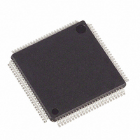
DS21Q50L Maxim Integrated Products, DS21Q50L Datasheet - Page 66

DS21Q50L
Manufacturer Part Number
DS21Q50L
Description
IC TRANSCEIVER E1 QUAD 100-LQFP
Manufacturer
Maxim Integrated Products
Datasheet
1.DS21Q50L.pdf
(87 pages)
Specifications of DS21Q50L
Function
Transceiver
Interface
E1
Number Of Circuits
4
Voltage - Supply
3.14 V ~ 3.47 V
Current - Supply
230mA
Operating Temperature
0°C ~ 70°C
Mounting Type
Surface Mount
Package / Case
100-LQFP
Includes
AIS Alarms Detector and Generator, Loopback Functions, PRBS Generator / Detector, Remote Detector and Generator
Lead Free Status / RoHS Status
Contains lead / RoHS non-compliant
Power (watts)
-
Available stocks
Company
Part Number
Manufacturer
Quantity
Price
Part Number:
DS21Q50L
Manufacturer:
MAXIM/美信
Quantity:
20 000
Company:
Part Number:
DS21Q50L+
Manufacturer:
SPANSION
Quantity:
119
Company:
Part Number:
DS21Q50L+
Manufacturer:
MAXIM
Quantity:
3
Company:
Part Number:
DS21Q50L-W+
Manufacturer:
Maxim Integrated
Quantity:
10 000
18.
In many architectures, the PCM outputs of individual framers are combined into higher speed PCM buses
to simplify transport across the system backplane. The DS21Q50 can be configured to allow PCM data
buses to be multiplexed into higher speed data buses, eliminating external hardware, saving board space
and cost. The DS21Q50 uses a channel interleave method. See
about the channel interleave.
The interleaved PCM bus option (IBO) supports three bus speeds. The 4.096MHz bus speed allows two
PCM data streams to share a common bus. The 8.192MHz bus speed allows four PCM data streams to
share a common bus. The 16.384MHz bus speed allows eight PCM data streams to share a common bus.
See
elastic stores of each transceiver must be enabled. Through the IBO register, the user can configure each
transceiver for a specific bus speed and position. For all IBO bus configurations, each transceiver is
assigned an exclusive position in the high-speed PCM bus. When the device is configured for IBO
operation, the TSYNCx pin should be configured as an output or as an input connected to ground. The
user cannot supply a TSYNCx signal in this mode.
Register Name:
Register Description:
Register Address:
Bit
Name
Table 18-1. IBO Device Assignment
IBOTCS
NAME
IBOEN
SCS1
SCS0
DA2
DA1
DA0
Figure 18-1
DA2
—
0
0
0
0
1
1
1
1
INTERLEAVED PCM BUS OPERATION
—
7
for an example of four transceivers sharing a common 8.192MHz PCM bus. The receive
DA1
BIT
IBOTCS
7
6
5
4
3
2
1
0
0
0
1
1
0
0
1
1
6
IBOR
Interleave Bus Operation Register
1C Hex
Not Assigned. Should be set to 0.
IBO Transmit Clock Source
0 = TCLK pin is the source of transmit clock
1 = transmit clock is internally derived from the clock at the SYSCLK pin
System Clock Select Bit 1
System Clock Select Bit 0
Interleave Bus Operation Enable
0 = interleave bus operation disabled
1 = interleave bus operation enabled
Device Assignment Bit 3
Device Assignment Bit 2
Device Assignment Bit 1
SCS1
DA0
5
0
1
0
1
0
1
0
1
SCS0
4
66 of 87
2nd Device on bus
3rd Device on bus
4th Device on bus
5th Device on bus
6th Device on bus
7th Device on bus
8th Device on bus
1st Device on bus
FUNCTION
(Table
(Table
(Table
(Table
(Table
IBOEN
3
18-1)
18-1)
18-1)
FUNCTION
18-2)
18-2)
Figure 19-4
DA2
2
and
DA1
1
Figure 19-7
DA0
for details
0


