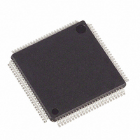
DS21Q50L Maxim Integrated Products, DS21Q50L Datasheet - Page 6

DS21Q50L
Manufacturer Part Number
DS21Q50L
Description
IC TRANSCEIVER E1 QUAD 100-LQFP
Manufacturer
Maxim Integrated Products
Datasheet
1.DS21Q50L.pdf
(87 pages)
Specifications of DS21Q50L
Function
Transceiver
Interface
E1
Number Of Circuits
4
Voltage - Supply
3.14 V ~ 3.47 V
Current - Supply
230mA
Operating Temperature
0°C ~ 70°C
Mounting Type
Surface Mount
Package / Case
100-LQFP
Includes
AIS Alarms Detector and Generator, Loopback Functions, PRBS Generator / Detector, Remote Detector and Generator
Lead Free Status / RoHS Status
Contains lead / RoHS non-compliant
Power (watts)
-
Available stocks
Company
Part Number
Manufacturer
Quantity
Price
Part Number:
DS21Q50L
Manufacturer:
MAXIM/ç¾ژن؟،
Quantity:
20 000
Company:
Part Number:
DS21Q50L+
Manufacturer:
SPANSION
Quantity:
119
Company:
Part Number:
DS21Q50L+
Manufacturer:
MAXIM
Quantity:
3
Company:
Part Number:
DS21Q50L-W+
Manufacturer:
Maxim Integrated
Quantity:
10 000
DS21Q50
1. INTRODUCTION
The DS21Q50 is optimized for high-density termination of E1 lines. Two significant features are included
for this type of application: the interleave bus option (IBO) and a system clock synthesizer feature. The
IBO allows up to eight E1 data streams to be multiplexed onto a single high-speed PCM bus without
additional external logic. The system clock synthesizer feature allows any of the E1 lines to be selected as
the master source of clock for the system and for all the transmitters. This is also accomplished without
the need of external logic. Each of the four transceivers has a clock and data jitter attenuator that can be
assigned to either the transmit or receive path. In addition there is a single, undedicated clock jitter
attenuator that can be hardware configured as the user needs. Each transceiver also contains a PRBS
pattern generator and detector.
Figure 18-1
shows a simplified typical application that terminates eight E1
lines (transmit and receive pairs) and combines the data into a single 16.384MHz PCM bus. The
16.384MHz system clock is derived and phased-locked to one of the eight E1 lines. On the receive side of
each port, an elastic store provides logical management of any slip conditions because of the
asynchronous relationship of the eight E1 lines. In this application, all eight transmitters are timed to the
selected E1 line.
The analog AMI/HDB3 waveform off of the E1 line is transformer coupled into the RRING and RTIP
pins of the DS21Q50. The device recovers clock and data from the analog signal and passes it through the
jitter attenuation mux to the receive framer where the digital serial stream is analyzed to locate the
framing/multiframe pattern. The DS21Q50 contains an active filter that reconstructs the analog received
signal for the nonlinear losses that occur in transmission. The device has a usable receive sensitivity of
0dB to -43dB, which allows the device to operate on cables over 2km in length. The receive framer
locates FAS frame and CRC and CAS multiframe boundaries as well as detects incoming alarms
including, carrier loss, loss of synchronization, AIS, and remote alarm. If needed, the receive elastic store
can be enabled in order to absorb the phase and frequency differences between the recovered E1 data
stream and an asynchronous backplane clock which is provided at the SYSCLK input. The clock applied
at the SYSCLK input can be either a 2.048MHz/4.096MHz/8.192MHz or 16.384MHz clock. The
transmit framer is independent from the receive in both the clock requirements and characteristics. The
transmit formatter provides the necessary frame/multiframe data overhead for E1 transmission.
6 of 87


