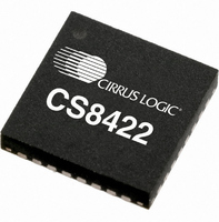
CS8422-CNZ Cirrus Logic Inc, CS8422-CNZ Datasheet - Page 12

CS8422-CNZ
Manufacturer Part Number
CS8422-CNZ
Description
IC SAMPLE RATE CONVERTER 32QFN
Manufacturer
Cirrus Logic Inc
Type
Sample Rate Converterr
Datasheet
1.CS8422-CNZ.pdf
(82 pages)
Specifications of CS8422-CNZ
Package / Case
32-QFN
Applications
Digital Audio
Mounting Type
Surface Mount
Maximum Operating Temperature
+ 125 C
Minimum Operating Temperature
- 55 C
Mounting Style
SMD/SMT
Package
32QFN
Operating Temperature
-55 to 125 °C
Audio Control Type
Sample Rate Converter
Control Interface
I2C, SPI
Supply Voltage Range
1.71V To 5.25V
Operating Temperature Range
-40°C To +85°C
Audio Ic Case Style
QFN
No. Of Pins
32
Rohs Compliant
Yes
Lead Free Status / RoHS Status
Lead free / RoHS Compliant
For Use With
598-1568 - BOARD EVAL FOR CS8422 RCVR
Lead Free Status / Rohs Status
Lead free / RoHS Compliant
Other names
598-1732
Available stocks
Company
Part Number
Manufacturer
Quantity
Price
Company:
Part Number:
CS8422-CNZ
Manufacturer:
CIRRUS
Quantity:
99
Part Number:
CS8422-CNZ
Manufacturer:
CIRRUS
Quantity:
20 000
Part Number:
CS8422-CNZR
Manufacturer:
CIRRUS
Quantity:
20 000
12
MCLK_OUT
TX_SEL
RX_SEL
RCBL
C
TX/U
V_REG
VD_FILT
DGND
VL
SDOUT2
OSCLK2
OLRCK2
TDM_IN
SDOUT1
OSCLK1
OLRCK1
SRC_UNLOCK
RMCK
RST
THERMAL PAD
Pin Name
Pin #
13
14
15
16
17
18
19
20
21
22
23
24
25
26
27
28
29
30
31
32
-
Buffered MCLK (Output) - Buffered output of XTI clock. If a 20 k pull-up resistor to VL is present on
this pin, the SRC MCLK source will be the PLL clock, otherwise it will be the ring oscillator.
TX Pin MUX Selection (Input) - Used to select the AES3-compatible receiver input for pass-through
to the TX pin.
Receiver MUX Selection (Input) - Used to select the active AES3-compatible receiver input.
Receiver Channel Status Block (Output) -Indicates the beginning of a received channel status
block. Will go high for one subframe during each Z preamble following the first detected Z preamble.
If no Z preamble is detected, output is indeterminate. See
Channel Status Data (Output) - Serial channel status data output from the AES3-compatible
receiver, clocked by the rising and falling edges of OLRCK2 in master mode. A 20 k pull-up resistor
to VL must be present on this pin to put the part in Hardware Mode.
Receiver MUX Pass-through/User Data (Output) - If no 20 k pull-up resistor is present on this pin
it will output a copy of the receiver mux input selected by the TX_SEL pin. If a 20 k pull-up resistor
to VL is present on this pin, it will output serial User data from the AES3 receiver, clocked by the rising
and falling edges of OLRCK2 in master mode.
Voltage Regulator In (Input) - Regulator power supply input, nominally +3.3 V.
Digital Voltage Regulator Out (Output) - Digital core voltage regulator output. Should be connected
to digital ground through a 10 µF capacitor. Cannot be used as an external voltage source.
Digital & I/O Ground (Input) - Ground for the I/O and core logic. AGND and DGND should be con-
nected to a common ground area under the chip.
Logic Power (Input) - Input/Output power supply, typically +1.8 V, +2.5 V, +3.3 V, or +5.0 V.
Serial Audio Output 2 Data Port (Output) - Audio data serial output 2 pin.
Serial Audio Output 2 Bit Clock (Input/Output) - Serial bit clock for audio data on the SDOUT2 pin.
Serial Audio Output 2 Left/Right Clock (Input/Output) - Word rate clock for the audio data on the
SDOUT2 pin.
Serial Audio Output 1 TDM Input (Input) - Time Division Multiplexing serial audio data input.
Grounded when not used. See
Serial Audio Output 1 Data Port (Output) - Audio data serial output 1 pin. A 20 k pull-up to VL
present on this pin will disable de-emphasis auto detect.
Serial Audio Output 1 Bit Clock (Input/Output) - Serial bit clock for audio data on the SDOUT1 pin.
Serial Audio Output 1 Left/Right Clock (Input/Output) - Word rate clock for the audio data on the
SDOUT1 pin.
SRC Unlock Indicator (Output) - Indicates when the SRC is unlocked. See
page 37
Recovered Master Clock (Output) - Recovered master clock from the PLL. Frequency is 128 x,
256 x, or 512 x Fs, where Fs is the sample rate of the incoming AES3-compatible data or ISCLK/64.
If a 20 k pull-up to VL is present on this pin, the SDOUT1 MCLK source will be RMCK, otherwise it
will be the clock input through XTI-XTO.
Reset (Input) - When RST is low the CS8422 enters a low power mode and all internal states are
reset. On initial power up RST must be held low until the power supply is stable and all input clocks
are stable in frequency and phase.
Thermal Pad - Thermal relief pad. Should be connected to the ground plane for optimized heat dissi-
pation.
for more details.
“Time Division Multiplexing (TDM) Mode” on page 27
Pin Description
Figure 19 on page 36
“SRC Locking” on
for more detail.
for details.
CS8422
DS692F1


