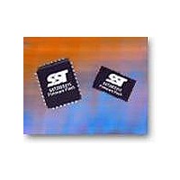
SST49LF016C-33-4C-WHE Microchip Technology, SST49LF016C-33-4C-WHE Datasheet - Page 9

SST49LF016C-33-4C-WHE
Manufacturer Part Number
SST49LF016C-33-4C-WHE
Description
IC FLASH SER LPC 16MBIT 32TSOP
Manufacturer
Microchip Technology
Datasheets
1.SST49LF080A-33-4C-NHE.pdf
(2 pages)
2.SST49LF080A-33-4C-NHE.pdf
(2 pages)
3.SST49LF016C-33-4C-NHE.pdf
(36 pages)
Specifications of SST49LF016C-33-4C-WHE
Memory Type
FLASH
Memory Size
16M (2M x 8)
Operating Temperature
0°C ~ 85°C
Package / Case
32-TSOP
Format - Memory
FLASH
Speed
33MHz
Interface
Parallel
Voltage - Supply
3 V ~ 3.6 V
Data Bus Width
8 bit
Architecture
Sectored
Interface Type
Parallel, Serial
Supply Voltage (max)
3.6 V
Supply Voltage (min)
3 V
Maximum Operating Current
18 mA
Mounting Style
SMD/SMT
Organization
4 KB x 512
Lead Free Status / RoHS Status
Lead free / RoHS Compliant
Lead Free Status / RoHS Status
Lead free / RoHS Compliant, Lead free / RoHS Compliant
Available stocks
Company
Part Number
Manufacturer
Quantity
Price
Company:
Part Number:
SST49LF016C-33-4C-WHE
Manufacturer:
Microchip Technology
Quantity:
135
16 Mbit LPC Serial Flash
SST49LF016C
Load Enable
The Load Enable pin (LD#), is an input pin which when low,
indicates the host is loading data in an AAI programming
cycle. Data is loaded in the SST49LF016C at the rising
edge of the clock. If LD# is high, it signals the AAI interface
that the host is terminating the command. LD# low/high
switches the RY/BY# output from buffer free flag to pro-
gramming complete flag (see Table 18).
No Connection (NC)
These pins are not connected internally.
DESIGN CONSIDERATIONS
SST recommends a high frequency 0.1 µF ceramic capac-
itor to be placed as close as possible between V
V
Additionally, a low frequency 4.7 µF electrolytic capacitor
from V
pin. If you use a socket for programming purposes add an
additional 1-10 µF next to each socket. The RST# pin must
remain stable at V
operation. WP#/AAI must remain stable at V
duration of the Erase and Program operations for non-Boot
Block sectors. To write data to the top Boot Block sectors,
the TBL# pin must also remain stable at V
duration of the Erase and Program operations.
MODE SELECTION
The SST49LF016C flash memory device operates in two
distinct interface modes: the LPC mode and the Auto
Address Increment (AAI) mode. The WP#/AAI pin is used
to set the interface mode selection. The device is in AAI
mode when the WP#/AAI pin is set to the Supervoltage V
(9±0.5V), and in the LPC mode when the WP#/AAI is set to
V
device operation.
©2008 Silicon Storage Technology, Inc.
SS
IL
/V
less than 1 cm away from the V
IH.
DD
The mode selection must be configured prior to
to V
SS
should be placed within 1 cm of the V
IH
for the entire duration of an Erase
DD
pin of the device.
IH
IH
for the entire
for the entire
DD
and
DD
H
9
LPC MODE
Device Operation
The SST49LF016C supports Multi-Byte Firmware Memory
Read and Write cycle types as defined in Low Pin Count
Interface Specification, Revision 1.1. Table 2 shows the
size of transfer supported by the SST49LF016C.
TABLE 2: Transfer Size Supported
The LPC mode uses a 5-signal communication interface:
one control line, LFRAME#, which is driven by the host to
start or abort a bus cycle, a 4-bit data bus, LAD[3:0], used
to communicate cycle type, cycle direction, ID selection,
address, data and sync fields. The device enters standby
mode when LFRAME# is taken high and no internal opera-
tion is in progress.
The host drives LFRAME# signal from low-to-high to cap-
ture the start field of a LPC cycle. On the cycle in which
LFRAME# goes inactive, the last latched value is taken as
the START value. The START value determines whether
the SST49LF016C will respond to a Firmware Memory
Read/Write cycle type as defined in Table 3.
TABLE 3: Firmware Memory Cycles START Field
See following sections on details of Firmware Memory
cycle types (Tables 4 and 5). Two-cycle Program and
Erase command sequences are used to initiate Firmware
Memory Program and Erase operations. See Table 8 for a
listing of Program and Erase commands.
Cycle Type
Firmware Memory Read
Firmware Memory Write
START
Value
1101
1110
Definition
Start of a Firmware Memory Read cycle
Start of a Firmware Memory Write cycle
Definition
Size of Transfer
1, 2, 4, 16, 128 Bytes
1, 2, 4 Bytes
S71237-08-000
Data Sheet
T2.1 1237
T3.1 1237
5/08


