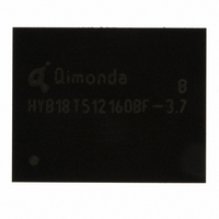
HYB18T1G160BF-5 Qimonda, HYB18T1G160BF-5 Datasheet - Page 49

HYB18T1G160BF-5
Manufacturer Part Number
HYB18T1G160BF-5
Description
IC DDR2 SDRAM 1GBIT 84TFBGA
Manufacturer
Qimonda
Datasheet
1.HYB18T1G800BF-3S.pdf
(74 pages)
Specifications of HYB18T1G160BF-5
Format - Memory
RAM
Memory Type
DDR2 SDRAM
Memory Size
1G (64M x 16)
Speed
200MHz
Interface
Parallel
Voltage - Supply
1.7 V ~ 1.9 V
Operating Temperature
0°C ~ 95°C
Package / Case
84-TFBGA
Lead Free Status / RoHS Status
Lead free / RoHS Compliant
Other names
675-1018-2
1)
2) Timing that is not specified is illegal and after such an event, in order to guarantee proper operation, the DRAM must be powered down
3) Timings are guaranteed with CK/CK differential Slew Rate of 2.0 V/ns. For DQS signals timings are guaranteed with a differential Slew
4) The CK / CK input reference level (for timing reference to CK / CK) is the point at which CK and CK cross. The DQS / DQS, RDQS / RDQS,
5) Inputs are not recognized as valid until
6) The output timing reference voltage level is
7) New units, ‘
8) When the device is operated with input clock jitter, this parameter needs to be derated by the actual
9) Input clock jitter spec parameter. These parameters and the ones in
Rev. 1.3, 2007-07
03062006-ZNH8-HURV
Parameter
DQ hold skew factor
Average periodic refresh Interval
Auto-Refresh to Active/Auto-Refresh command
period
Precharge-All (8 banks) command period
Read preamble
Read postamble
Active to active command period for 1KB page
size products
Active to active command period for 2KB page
size products
Internal Read to Precharge command delay
Write preamble
Write postamble
Write recovery time
Internal write to read command delay
Exit power down to read command
Exit active power-down mode to read command
(slow exit, lower power)
Exit precharge power-down to any valid
command (other than NOP or Deselect)
Exit self-refresh to a non-read command
Exit self-refresh to read command
Write command to DQS associated clock edges
V
and then restarted through the specified initialization sequence before normal operation can continue.
Rate of 2.0 V/ns in differential strobe mode and a Slew Rate of 1 V/ns in single ended mode.
input reference level is the crosspoint when in differential strobe mode. The input reference level for signals other than CK/CK, DQS/DQS,
RDQS / RDQS is defined.
under operation. Unit ‘nCK‘ represents one clock cycle of the input clock, counting the actual clock edges. Note that in DDR2–400 and
DDR2–533, ‘
may be registered at Tm + 2, even if (Tm + 2 - Tm) is 2 x
deratings are relative to the SDRAM input clock.) For example, if the measured jitter into a DDR2–667 SDRAM has
– 272 ps and
t
= - 900 ps – 293 ps = – 1193 ps and
these parameters apply to DDR2–667 and DDR2–800 only. The jitter specified is a random jitter meeting a Gaussian distribution.
DQSCK.MAX(DERATED)
DDQ
= 1.8 V ± 0.1V;
t
CK.AVG
t
CK
t
ERR(6- 10PER).MAX
‘ is used for both concepts. Example:
‘ and ‘nCK‘, are introduced in DDR2–667 and DDR2–800. Unit ‘
=
t
V
DQSCK.MAX
DD
= 1.8 V ± 0.1 V.
= + 293 ps, then
–
t
ERR(6-10PER).MIN
t
LZ.DQ.MAX(DERATED)
V
REF
V
stabilizes. During the period before
TT
t
.
DQSCK.MIN(DERATED)
= 400 ps + 272 ps = + 672 ps. Similarly,
t
Symbol
t
t
t
t
t
t
t
t
t
t
t
t
t
t
t
t
t
t
WL
XP
QHS
REFI
RFC
RP
RPRE
RPST
RRD
RRD
RTP
WPRE
WPST
WR
WTR
XARD
XARDS
XP
XSNR
XSRD
= 450 ps + 272 ps = + 722 ps. (Caution on the MIN/MAX usage!)
= 2 [nCK] means; if Power Down exit is registered at Tm, an Active command
t
CK.AVG
+
49
=
t
t
ERR.2PER(Min)
Chapter 7.3
DQSCK.MIN
DDR2–800
—
—
—
127.5
t
0.9
0.4
7.5
10
7.5
0.35
0.4
15
7.5
2
8 – AL
2
t
200
RL – 1
Min.
RP
RFC
+ 1 ×
+10
–
.
t
ERR(6-10PER).MAX
V
are referred to as 'input clock jitter spec parameters' and
REF
t
t
CK.AVG
CK
stabilizes, CKE = 0.2 x
t
1-Gbit Double-Data-Rate-Two SDRAM
‘ represents the actual
LZ.DQ
—
1.1
0.6
—
—
—
—
0.6
—
—
—
—
—
—
Max.
300
7.8
3.9
—
—
HY[B/I]18T1G[40/80/16]0B[C/F](L/V)
for DDR2–667 derates to
= – 400 ps – 293 ps = – 693 ps and
t
ERR(6-10per)
V
Unit
ps
µs
µs
ns
ns
t
t
ns
ns
ns
t
t
ns
ns
nCK
nCK
nCK
ns
nCK
nCK
CK.AVG
CK.AVG
CK.AVG
CK.AVG
DDQ
of the input clock. (output
t
Internet Data Sheet
CK.AVG
is recognized as low.
t
ERR(6-10PER).MIN
of the input clock
Note
26)
27)28)
28)29)
30)
31)32)
31)33)
34)
34)
34)
34)
34)35)
34)
t
LZ.DQ.MIN(DERATED)
1)2)3)4)5)6)7)
=


