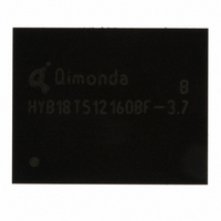
HYB18T1G160BF-5 Qimonda, HYB18T1G160BF-5 Datasheet - Page 51

HYB18T1G160BF-5
Manufacturer Part Number
HYB18T1G160BF-5
Description
IC DDR2 SDRAM 1GBIT 84TFBGA
Manufacturer
Qimonda
Datasheet
1.HYB18T1G800BF-3S.pdf
(74 pages)
Specifications of HYB18T1G160BF-5
Format - Memory
RAM
Memory Type
DDR2 SDRAM
Memory Size
1G (64M x 16)
Speed
200MHz
Interface
Parallel
Voltage - Supply
1.7 V ~ 1.9 V
Operating Temperature
0°C ~ 95°C
Package / Case
84-TFBGA
Lead Free Status / RoHS Status
Lead free / RoHS Compliant
Other names
675-1018-2
32) When the device is operated with input clock jitter, this parameter needs to be derated by the actual
33) When the device is operated with input clock jitter, this parameter needs to be derated by the actual
34) For these parameters, the DDR2 SDRAM device is characterized and verified to support
35)
Rev. 1.3, 2007-07
03062006-ZNH8-HURV
Parameter
DQ output access time from CK / CK
CAS to CAS command delay
Average clock high pulse width
Average clock period
CKE minimum pulse width ( high and low pulse
width)
Average clock low pulse width
Auto-Precharge write recovery + precharge time
Minimum time clocks remain ON after CKE
asynchronously drops LOW
DQ and DM input hold time
DQ and DM input pulse width for each input
DQS output access time from CK / CK
DQS input high pulse width
DQS input low pulse width
DQS-DQ skew for DQS & associated DQ signals
DQS latching rising transition to associated clock
edges
DQ and DM input setup time
DQS falling edge hold time from CK
DQS falling edge to CK setup time
Four Activate Window for 1KB page size products
Four Activate Window for 2KB page size products
CK half pulse width
Data-out high-impedance time from CK / CK
Address and control input hold time
deratings are relative to the SDRAM input clock.) For example, if the measured jitter into a DDR2–667 SDRAM has
and
+
deratings are relative to the SDRAM input clock.) For example, if the measured jitter into a DDR2–667 SDRAM has
and
+
cycles, assuming all input clock jitter specifications are satisfied. For example, the device will support
clock cycles, if all input clock jitter specifications are met. This means: For DDR2–667 5–5–5, of which
t
Tm + 5 is valid even if (Tm + 5 - Tm) is less than 15 ns due to input clock jitter.
t
nRP
WTR
t
t
JIT.PER.MAX
JIT.DUTY.MAX
t
t
= RU{
is at lease two clocks (2 x
JIT.PER.MAX
JIT.DUTY.MAX
t
RP
= 1.1 x
/
= 0.6 x
= + 93 ps, then
t
CK.AVG
= + 93 ps, then
t
CK.AVG
t
} = 5, i.e. as long as the input clock jitter specifications are met, Precharge command at Tm and Active command at
CK.AVG
+ 93 ps = + 2843 ps. (Caution on the MIN/MAX usage!).
+ 93 ps = + 1592 ps. (Caution on the MIN/MAX usage!).
t
RPRE.MIN(DERATED)
t
t
RPST.MIN(DERATED)
CK
) independent of operation frequency.
=
DRAM Component Timing Parameter by Speed Grade - DDR2–667
=
t
RPRE.MIN
t
RPST.MIN
Symbol
t
t
t
t
t
t
t
t
t
t
t
t
t
t
t
t
t
t
t
t
t
t
t
AC
CCD
CH.AVG
CK.AVG
CKE
CL.AVG
DAL
DELAY
DH.BASE
DIPW
DQSCK
DQSH
DQSL
DQSQ
DQSS
DS.BASE
DSH
DSS
FAW
FAW
HP
HZ
IH.BASE
+
+
t
JIT.PER.MIN
t
JIT.DUTY.MIN
51
= 0.9 x
= 0.4 x
DDR2–667
–450
2
0.48
3000
3
0.48
WR +
t
t
175
0.35
–400
0.35
0.35
—
– 0.25
100
0.2
0.2
37.5
50
Min(
t
—
275
Min.
IS
IH
CL.ABS
+
t
t
t
CK.AVG
CK .AVG
CH.ABS
t
)
CK.AVG
t
nRP
– 72 ps = + 2178 ps and
,
– 72 ps = + 928 ps and
+
1-Gbit Double-Data-Rate-Two SDRAM
t
nPARAM
+450
—
0.52
8000
—
0.52
––
—
+400
—
—
––
—
—
—
—
—
Max.
—
––
240
+ 0.25
__
t
HY[B/I]18T1G[40/80/16]0B[C/F](L/V)
AC.MAX
= RU{
t
t
JIT.PER
JIT.DUTY
t
t
nRP
RP
t
PARAM
= 15 ns, the device will support
= RU{
of the input clock. (output
t
of the input clock. (output
t
RPRE.MAX(DERATED)
RPST.MAX(DERATED)
Unit
ps
nCK
t
ps
nCK
t
nCK
ns
ps
t
ps
t
t
ps
t
ps
t
t
ns
ns
ps
ps
ps
/
CK.AVG
CK.AVG
CK.AVG
CK.AVG
CK.AVG
CK.AVG
CK.AVG
CK.AVG
t
CK.AVG
t
Internet Data Sheet
RP
/
t
t
JIT.DUTY.MIN
JIT.PER.MIN
t
TABLE 54
CK.AVG
}, which is in clock
Note
8)
9)10)
11)
9)10)
12)13)
18)19)14)
8)
15)
16)
17)18)19)
16)
16)
34)
34)
20)
8)21)
24)22)
}, which is in
1)2)3)4)5)6)7)
=
=
= – 72 ps
= – 72 ps
t
t
RPRE.MAX
RPST.MAX


